Service Manuals, User Guides, Schematic Diagrams or docs for : ONKYO Audio ds575dsp_01
<< Back | HomeMost service manuals and schematics are PDF files, so You will need Adobre Acrobat Reader to view : Acrobat Download Some of the files are DjVu format. Readers and resources available here : DjVu Resources
For the compressed files, most common are zip and rar. Please, extract files with Your favorite compression software ( WinZip, WinRAR ... ) before viewing. If a document has multiple parts, You should download all, before extracting.
Good luck. Repair on Your own risk. Make sure You know what You are doing.
Image preview - the first page of the document
>> Download ds575dsp_01 documenatation <<
Text preview - extract from the document
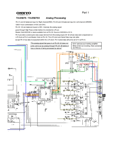
                                                                                                  Part 1

 TX-DS575 TX-DS575X
 TX DS575 / TX DS575X                        Analog Processing
Pin 31 and 32 balanced input for Right channel(RED); Pin 29 and 30 balanced input for Left channel (
                         p         g          (   )                           p                    (GREEN)
                                                                                                         )
Q8501 have combination of ADC and DAC.
Pin 29 ~32 are balanced inputs to ADC. Internaly the analog signal
g
goes through High Pass Limiter before it is clocked to L/R out.
          g    g
Master Clock MCK02 is made available from at Pin 39. Source of MCK02 is Q114.
Pin 9 provides a serial audio data output derived from the analog inputs 29~32 whose data rate is dependant on
L/R Clock at Pin 5 and Master Clock at Pin 39. The L/R clock and Serial Data may look alike
except Pin 9 has data incorpoarted within the L/R clock. Pin 9 serial data will arrive at Q114 at Pin 8.

                      "The analog signal that goes in at Pin 29~32 does not
                       The                                   29 32                  Q101 services as inverting amplifier
                      come come out as analog through Pin 23~28 before it
                                                          23 28                     While Q102 non inverting. Note correction
                      has a c a ce o be g p ocessed as abo e
                       as chance of being processed    above"                       On PIN 5,6,.


                                                                                                 6         6
                                                                                                 5         5
TX-DS575 TX-DS575X
TX DS575 / TX DS575X                               Analog Processing
 Audio Data f
            from Q8501 Pin 9 arrives at Pin 8 of Q114.
                 Q                             fQ                        Part 2
Same data will find its way out at pin 20 of Q114.
It is important X0-XI Pin 5 and Pin 6 work correct and that 12 2Mhz
                X0 XI     5,and                             12.2Mhz
 oscilation is present No noticable drift or Jitter should be noticed
               present.                                       noticed.
                                   TX-DS575 / TX-DS575X          ANALOG PROCESSING                           Part 3
  Analog                 Digital
Q114 Pin 15 = L            =H
                            H
 Q114 Pin 17 = H              =L
It is conditional that audio data is present at Pin 8 (DAUX) of Q114 and that X-tal X103 is ON in-order for Q114
 to operate properly The digital condition set forth at Pin 15 and 17 along a precence of digita data
             properly.
at Pin 13, 12 and 11 will turn OFF X103.


                                                                     4.6vdc


                   Q114 waveforms when input is analog.


                                                                                                       Q114 Pin 27
                                                                                                       when digital selected and
                                                                                                       digital signal detected.


  MCK01,MCK02 at Q114 Pin 24 & 23                       MCK01, MCK02 after L171 &L170


                                                                                                                   Pin 26 digital source
                                     Pin 19                                                                        selected. Absent when
                                     LRCK                                                                                g
                                                                                                                   analog.
TXDS575

                                                                                         Compiled on 05/24/2000
This is a part of more technical information to follow.

To help troubleshoot this model for audio related problem the following easy to follow method has been adapted.
Problem: Audio Analog via any source goes in and no audio out. Unit is not in protection mode.

       1. Assuming that you have signal present at the CD input, we will chase the signal as follows. When we do,
           we will consider all supply voltages are up and up. No ripple voltage is seen over the DC supply line.
       2. Remove the DSP PCB and set it flat with the component side accessible. Check for signal at pin 2 and 6, of
           Q101 and Q102. Please note that the pin label of Q101 and Q102 is incorrect. Pin 1 and 7 are output of
           those same IC's.
       3. Balanced output of Q101 and Q102 arrive at pin 29,30,31 and 32.
       4. Check for Master clock at Pin 39 of Q8501. If NO...
       5. Go and check Q114 pin 5 and 6 Xtal. If OK got to 6. If NO Q114 or X is not working. Replace Q114 and
           X103.
       6. Check Pin 23 and 24 to see if MCKO2 and MCK01 are running. If YES ...
       7. Check for data out at pin 9 of Q8501. If YES ...
       8. Check for the data again at pin 8 of Q114. If YES...
       9. Look for the data return at pin 20 and sample rate at pin 19. If NO Q114 is possibly defective.
       10. Pin 19 through 23 of Q114 working no Audio. Check for data present at pin 22 of Q707. If OK...
       11. Check for DC state at connector P7001A "AMUT". If high (>.400vdc) go back to DSP pin 30 of Q707.
           This point also should have a clock coming from Q702 pin 5. If NO...
       12. Check for the ripple voltage level on this IC Q702 and condition of X701 oscillation level. No distortion
           allowed. If NO ... check Q702 for defect or X701. Replace.
       13. If pin 5 of Q702 is good, Check DC voltage of Q707 pin 8,9,10,11,14,15,16,17 (8bit line) to the memory IC
           Q710. They should all read equal and just about 3.4Vdc. Data on all pins should be identical. If not Q710 i s
           defective with Q708 and Q709 on suspect list. It is also worth noting that before assuming Q710, Q708,
           Q709 is bad, check for broken or loose R7711 through R7718.
       14. When normal the following DC voltages appear at the following pins. See chart. Input is DVD digital set
           for PCM output or a CD player can be used.

                         Q707 operating as PCM, digital input.
                                    Pin#    01    02   03    04     05      06     07     08     09      10     11
                                  DC volt   3.3   0    0     0      3.3     0      0      3.3    3.3     3.3    3.3
                                    Pin#    12    13   14    15     16      17     18     19     20      21     22
                                  DC volt   3.3   0    3.3   3.3    3.3     3.3    4.8    3.3    4.9     3.3    .9
                                    Pin#    23    24   25    26     27      28     29     30     31      32     33
                                  DC volt   3.3   0    1.7   1.7    .9      1.7    1.7    1.7    0       2.8    2.2
                                    Pin#    34    35   36    37     38      39     40     41     42      43     44
                                  DC volt   3.4   0    4.8   3.3    3.3     1.1    1      1      1.7     1.7    1.7
Input Coax 1
Setting Digital

Q114 pin reference as follows.

X103 is off since input is digital.
Fig1


                              Pin 12 data is OK
Fig2:          Pin 26 and 27 clock is OFF when digital signal is present at pin 12.
               Pin 15 has no signal.

        Fig2


                      Data is present at pin 20. (.15us)                Without input signal (.6us)
                   Pin 19 and pin 20 appears like this when signal is present at pin 12


                      Q114, pin 23 and 24 clock is present and appears normal.


X701 is oscillating and is within spec12.2Mhz

Q707 (problem begins to show at:)

Pin 39 and 41 has no data.

                                              Pin 30 appears this way.
Pin 29


                                Pin 41 has a problem as seen. This point is
                                normally 4.5vpp rather than .636vpp. The data
                                appears to be corrupted or very low. If the unit
                                is working properly this point becomes very
                                high and clear data is present. At the same time
                                when the unit appears to work, Q707
                                temperature runs wormer than when it is not.


At this point a re-check of pin 8 through 17 reveled that some of the data line DC voltages were
not as they should be. See chart.

Q710 Defective. Replaced and unit worked.
◦ Jabse Service Manual Search 2024 ◦ Jabse Pravopis ◦ onTap.bg ◦ Other service manual resources online : Fixya ◦ eServiceinfo