Service Manuals, User Guides, Schematic Diagrams or docs for : Agilent HP 8663A Service Vol 2
<< Back | HomeMost service manuals and schematics are PDF files, so You will need Adobre Acrobat Reader to view : Acrobat Download Some of the files are DjVu format. Readers and resources available here : DjVu Resources
For the compressed files, most common are zip and rar. Please, extract files with Your favorite compression software ( WinZip, WinRAR ... ) before viewing. If a document has multiple parts, You should download all, before extracting.
Good luck. Repair on Your own risk. Make sure You know what You are doing.
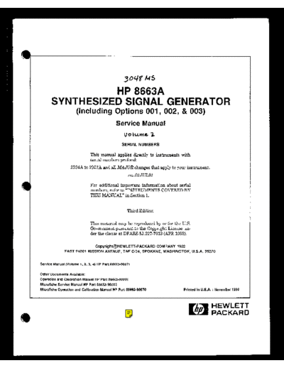
Image preview - the first page of the document

>> Download HP 8663A Service Vol 2 documenatation <<
Text preview - extract from the document
                                     3wr        Ads
           HP 8663A
SYNTHESIZED SIGNAL GENERATOR
        (Including               Options         001, 002, & 003)
                                 Service Manual
                                   v01uw& TiL
                                    SERIAL   NUMBERS

                     This manual appliesdkectly to instrumentswith
                     serialnumberspr&xedz
     2234A     to   2927A andall MAJORchanges    that applyto your imtrument.
                                       rw. 0.l JUL91

                     For additionalimpm-tantinformation aboutserial
                     mmbers,refer to ~INSTRUMENTS    COVERED   BY
                     THE? MANUAL" in Section  1.

                                       Third Edition

                     This materialmay bs reproduced or for the U.S.
                                                   by
                     Government  pursuantto the CopytightLicenseWI-
                     der the clause l3Fm 52.227-7013 1988).
                                  at                   UPR

                        Copyright@HEWLETT-PACKARD   COMPANY    1982
  EAST 24001        MISSION AVENUE, TAF G34, SPOKANE,  WASIIINGTON,    U.S.A.    99220


                                                                  Prhted   I" lJ.s.*.   : No"elnner   two


                                                                                        HEWLETT
                                                                                        PACKARD
                    COPYRIGHT AND DISCLAIMER NOTICE

Copyright - Agilent Technologies, Inc. Reproduced with the permission of Agilent
Technologies Inc. Agilent Technologies, Inc. makes no warranty of any kind with regard
to this material including, but not limited to, the implied warranties of merchantability
and fitness for a particular purpose. Agilent Technologies, Inc. is not liable for errors
contained herein or for incidental or consequential damages in connection with the
furnishing, performance, or use of this material or data.
Model 8663A                                                                                                      Volume 2 ConteIlti


                               VOLUME 2 CONtENTS

 SCheimzULz                                                                                        Theory/Trouble-         Pan*
  salvica       Mock                       Assembly        or SectIon                                  ShootinS             List
   Sheet      Diagram                                                                                     Page             Page
  Number                                                                                               Number             Number

    SD1          -             Overall     Block Diagram         (Instrument      Level)                 a-201
    602          -             uefersnce       secuoll                                                   6-21.3              -

    SD3          -             High Frsquency            Lcops   Section                                 e-217               -

    BD4          -             FrsctiOnal-N       Loops     Section                                      6-223
    BD5          -             Low Prequency           Loops     Section                                 6-235               -

    BD6                        output      saction                                                       0-241               -

    SD7          -             ModulaUon        Section                                                  6-249               -

    SD8          -             Phase     Modulation        Ssction                                       6-257               -

    BD9          -             DigItsI control       unit (DCU) section                                  E-261
   SD10          -             pdwsr     Supply      Section                                            6-269                -

    SSl         ED2     AM3    10 MHz Reference             Oscklator                                   6-301              6-i 76
                SD2     A6A4   Referenca Buff.sr

    ss2         BD2     A6Al   Referents       Section      LF MultIplier                               e-307              6-117
    ss3         BD2     AM3    Referwwe        Section      HF MultIplier                               6-313              6-l 25
    ss4         SD2     A6A2   Reference       Section      LO Drive                                    5319               6-121
    SS5        BD3      A6A9   HP Loops       and Reference           SectIons    controller            6-325              6-l 55

   SS6         BD3      A6A6   Fwferencs      Sum Loop RF Mixw                                          e-331              6-149
   ss7         SD3      AM5    Rafwonce       Sum Loop Phase               Detector                     a-337              E-133
   SS8         BD3      A6A5   Reference      Sum Loop Phase               Detector                     6-347              6-133
   ss9         SD3      A6A7   RF Buffsr                                                                6-355              6-151
   SSlO        BD3      A6A6   Output    Sum Loop RF Mlxsr                                              6-361              6-153
   s.C.11      SD3      A6A4   Output    Sum Loop Phase Detector                                        6-367              6-133
   SW2         BD3      ABA4   Output    Sum Loop Phase Detector                               '        .9-w7              6-l 33


rm3OSEP88
Model 8663A                                                                      Service


SERVICE SHEET BDl
OVERALL BLOCK DIAGRAM

REFERENCE:
   Simplified        Operation   (Sec'tion III)
   Opera't~r~s       Checks (Section III)
   Table 4-l.        Recommended Performance Tests
                     After Adjustments     or Repairs.
      Table   5-2.   Post-Repair   Adjustment Procedures

PRINCIPLES OF OPERATION
The basic frequency      generating       circuitry      is composed of the Reference
Section,   phase lock loops and Output Section (in the upper-left>                  aenter
and right    hand portions      of the block diagram respectively).                 All of
the reference    frequencies     used within         the instrument    are obtained    from
the Reference Section.       A total     of seven phase lock loops work together
.Lo produce the fundamental          fre'quency band of 320 'to 640 MHz with a
step resolution      of 0.1 Hz. This fundamental               (or basic)  band is SW-t
to the Output Section where it is doubled, passed straight                     through or
down-converted     to produce the entire            frequency    range at the RF output
(.l   to   2560   MHZ).
The Digi,tal     Control   Unit  (DCU) controls      the operation     of the unit.
It accepts keyboard or remote inputs and generates               internal   data and
control    signals   to control   the signal at the RF output.         Power for the
instrument     is supplied   by a switching-regulated     power supply.

Reference       Section
AlI     of   the reference        frequencies        used within    the instrument    are
obtained from the Reference Section.                This block is composed of doublers,
dividers,       and mixers,    all of which are driven by a single temperature-
s,tabilized      10 MHz crystal     oscillator.      Outputs from the Reference Section
are   10,   20,   120,  520,  and 320-640 MHZ (in 20 MHz steps).           Signal levels
vary depending on which section                 they are being sent to.

Phase Lock Loops
'The Generator uses the indirect     synthesis   method for generating    output
l'requencies.  Phase lock loop (PLL) circuits       are locked to signals    from
the Reference Section and generate signals which are combined to giv@
the desired   output   frequency,   All output frequencies     retain  the same
accuracy and stability      as the 1C MHz reference    signal.  PLL's are found
in ,the IHigh Frequency,      Low Frequency,   Fractional-N,    and Modulation
Sections.
◦ Jabse Service Manual Search 2024 ◦ Jabse Pravopis ◦ onTap.bg ◦ Other service manual resources online : Fixya ◦ eServiceinfo