Service Manuals, User Guides, Schematic Diagrams or docs for : Chroma 63103a AD7537
<< Back | HomeMost service manuals and schematics are PDF files, so You will need Adobre Acrobat Reader to view : Acrobat Download Some of the files are DjVu format. Readers and resources available here : DjVu Resources
For the compressed files, most common are zip and rar. Please, extract files with Your favorite compression software ( WinZip, WinRAR ... ) before viewing. If a document has multiple parts, You should download all, before extracting.
Good luck. Repair on Your own risk. Make sure You know what You are doing.
Image preview - the first page of the document
>> Download AD7537 documenatation <<
Text preview - extract from the document
a LC2MOS
(8+4) Loading Dual 12-Bit DAC
AD7537
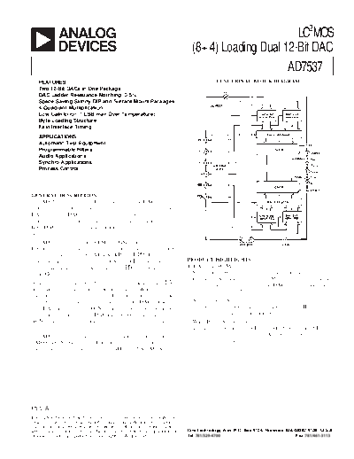
FEATURES FUNCTIONAL BLOCK DIAGRAM
Two 12-Bit DACs in One Package
DAC Ladder Resistance Matching: 0.5%
Space Saving Skinny DIP and Surface Mount Packages
4-Quadrant Multiplication
Low Gain Error (1 LSB max Over Temperature)
Byte Loading Structure
Fast Interface Timing
APPLICATIONS
Automatic Test Equipment
Programmable Filters
Audio Applications
Synchro Applications
Process Control
GENERAL DESCRIPTION
The AD7537 contains two 12-bit current output DACs on one
monolithic chip. A separate reference input is provided for each
DAC. The dual DAC saves valuable board space, and the
monolithic construction ensures excellent thermal tracking.
Both DACs are guaranteed 12-bit monotonic over the full tem-
perature range.
The AD7537 has a 2-byte (8 LSBs, 4 MSBs) loading structure.
It is designed for right-justified data format. The control signals
for register loading are A0, A1, CS, WR and UPD. Data is
loaded to the input registers when CS and WR are low. To PRODUCT HIGHLIGHTS
transfer this data to the DAC registers, UPD must be taken low 1. DAC to DAC Matching:
with WR. Since both DACs are fabricated on the same chip, precise
matching and tracking is inherent. Many applications which
Added features on the AD7537 include an asynchronous CLR are not practical using two discrete DACs are now possible.
line which is very useful in calibration routines. When this is Typical matching: 0.5%.
taken low, all registers are cleared. The double buffering of the
data inputs allows simultaneous update of both DACs. Also, 2. Small Package Size:
each DAC has a separate AGND line. This increases the device The AD7537 is packaged in small 24-pin 0.3" DIPs and in
versatility; for instance one DAC may be operated with 28-terminal surface mount packages.
AGND biased while the other is connected in the standard 3. Wide Power Supply Tolerance:
configuration. The device operates on a +12 V to +15 V VDD, with ◦ Jabse Service Manual Search 2024 ◦ Jabse Pravopis ◦ onTap.bg ◦ Other service manual resources online : Fixya ◦ eServiceinfo