Service Manuals, User Guides, Schematic Diagrams or docs for : DENON Audio DN-X300 DENON DN-X300+Mixer+audio

<< Back | Home

Most service manuals and schematics are PDF files, so You will need Adobre Acrobat Reader to view : Acrobat Download Some of the files are DjVu format. Readers and resources available here : DjVu Resources
For the compressed files, most common are zip and rar. Please, extract files with Your favorite compression software ( WinZip, WinRAR ... ) before viewing. If a document has multiple parts, You should download all, before extracting.
Good luck. Repair on Your own risk. Make sure You know what You are doing.


Image preview - the first page of the document
DENON DN-X300+Mixer+audio


>> Download DENON DN-X300+Mixer+audio documenatation <<

Text preview - extract from the document
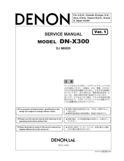
                                                              For U.S.A., Canada, Europe, U.K.,
                                                              Asia, China, Taiwan R.O.C., Korea
                                                              & Japan model


                                                                                Ver. 1
                               SERVICE MANUAL
                      MODEL                       DN-X300
                                             DJ MIXER


For purposes of improvement, specifications and
design are subject to change without notice.


Please use this service manual with referring to the
operating instructions without fail.


Some illustrations using in this service manual are
slightly different from the actual set.


                                               TOKYO, JAPAN


                                                                                 X0212V.01 DE/CDM 0408
                                                                                                                 DN-X300


SAFETY PRECAUTIONS
The following check should be performed for the continued protection of the customer and service technician.

LEAKAGE CURRENT CHECK
Before returning the unit to the customer, make sure you make either (1) a leakage current check or (2) a line to chassis
resistance check. If the leakage current exceeds 0.5 milliamps, or if the resistance from chassis to either side of the
power cord is less than 460 kohms, the unit is defective.


                                                                        500V


                                                                                            1M


(1)


(2)


                                                                 (1)

                                                                 (2)


                                                           2
                                                                   DN-X300


DISASSEMBLY
(Follow the procedure below in reverse order when reassembling.)

 1. Top Panel
  (1) Pull out the Knobs from the Top Panel.
  (2) Remove the 6 screws attaching the Top Panel.
  (3) Pull up the Front Panel.


    Note:
       Be careful in the attachment direction.


                                                             3
                                                                   DN-X300

2. Crossfader Unit
(1) Remove the 2 screws attaching the Crossfader Unit.
(2) Pull up the Crossfader Unit and disconnect the connector.


 Note:
    Be careful in the attachment direction.

3. Channel Fader Unit
(1) Remove the 3 screws attaching the Channel Fader Unit.
(2) Pull up the Channel Fader Unit and disconnect the connector.


                                                            4
                                                                     DN-X300

4. Input Selector Unit
 (1) Remove the 2 screws attaching the Input Selector Unit.
 (2) Pull up the Input Selector Unit and disconnect the connector.


  Note:
     Be careful in the attachment direction.

5. Top Panel Unit
 (1) Remove the 6 screws from the both-sides side.
 (2) Remove the 2 screws from the rear side.
 (3) Remove the 5 screws from the front side.
 (4) Remove the 4 screws from the bottom side.
 (5) Pull up the front side of the Top Unit.
 (6) Disconnect the connectors.


                                                              5
                    DN-X300


BLOCK DIAGRAM


                6
                                                                                                                               DN-X300


 Only major semiconductors are shown, general semiconductors etc. are omitted to list.


 1. IC's
       MAX003 (IC801)
                                                75                                          51
                                          76                                                     50


                                          100                                                    26
                                                 1                                          25

MAX003 Terminal Function

 Pin
        Pin Name    Symbol   I/O    Det   Int Pu     Ext   Res   Ini                                    Function
 No.
                                                                          VCL(capacitor between this pin and GND)in 5V operation models,and
 1      VCL        VCL         -     -      -         -     -     -
                                                                          as Vcc in 3V operation models.
 2      PB0        CH1FS       I     -      -        Pu     L    H        CH1 FADER START SW 'L' : ON
 3      PB1        PB1        O      -      -        Pu     L    L        Not used
 4      PB2        PB2        O      -      -        Pu     L    L        Not used
 5      PB3        PB3        O      -      -        Pu     L    L        Not used
 6      PB4        PB4        O      -      -        Pu     L    L        Not used
 7      PB5        PB5        O      -      -        Pu     L    H        Not used
 8      PB6        FX2SW       I     -      -        Pu     L    H        PGM2 EFFECT LOOP ON/OFF SW 'L' : ON (DN-X300 only)
 9      PB7        CHREV       I     -      -        Pu     L    H        CH REVERSE SW 'L' : ON
 10     _RESO      _RESO      O      -      -         -     -     -       Not used
 11     Vss        Vss         -     -      -         -     -     -       GND(0V)
 12     P90        P90        O      -      -         -     L    L        Not used
 13     P91        P91        O      -      -         -     L    L        Not used
 14     P92        P92        O      -      -         -     L    L        Not used
 15     P93        P93        O      -      -         -     L    L        Not used
 16     P94        P94        O      -      -         -     L    L        Not used
 17     P95        P95        O      -      -         -     L    L        Not used
 18     P40        P40        O      -     ON         -     L    L        Not used
 19     P41        P41        O      -     ON         -     L    L        Not used
 20     P42        P42        O      -     ON         -     L    L        Not used
 21     P43        PC1A      I/O     -     ON         -     L    H        PGM1 Fader PLAY output 30msec 'L' pulse
 22     Vss        Vss         -     -      -         -     -     -       GND(0V)
 23     P44        PC1B      I/O     -     ON         -     L    H        PGM1 Fader CUE output       30msec 'L' pulse
 24     P45        PC2A      I/O     -     ON         -     L    H        PGM2 Fader PLAY output 30msec 'L' pulse
 25     P46        PC2B      I/O     -     ON         -     L    H        PGM2 Fader CUE output       30msec 'L' pulse
 26     P47        P47        O      -     ON         -     L    L        Not used
 27     D8         D0         D/I    -      -         -     -     -       Data bus
 28     D9         D1         D/I    -      -         -     -     -       Data bus
 29     D10        D2         D/I    -      -         -     -     -       Data bus
 30     D11        D3         D/I    -      -         -     -     -       Data bus
 31     D12        D4         D/I    -      -         -     -     -       Data bus
 32     D13        D5         D/I    -      -         -     -     -       Data bus


                                                                      7
                                                                                                                                 DN-X300


Pin
      Pin Name     Symbol   I/O   Det   Int Pu   Ext   Res   Ini                                     Function
No.
33    D14        D6         D/I    -      -       -     -     -       Data bus
34    D15        D7         D/I    -      -       -     -     -       Data bus
35    Vcc        Vcc         -     -      -       -     -     -       Power supply(+5V)
36    A0         A0         A/O    -      -       -     -     -       Address bus
37    A1         A1         A/O    -      -       -     -     -       Address bus
38    A2         A2         A/O    -      -       -     -     -       Address bus
39    A3         A3         A/O    -      -       -     -     -       Address bus
40    A4         A4         A/O    -      -       -     -     -       Address bus
41    A5         A5         A/O    -      -       -     -     -       Address bus
42    A6         A6         A/O    -      -       -     -     -       Address bus
43    A7         A7         A/O    -      -       -     -     -       Address bus
44    Vss        Vss         -     -      -       -     -     -       GND(0V)
45    A8         A8         A/O    -      -       -     -     -       Address bus
46    A9         A9         A/O    -      -       -     -     -       Address bus
47    A10        A10        A/O    -      -       -     -     -       Address bus
48    A11        A11        A/O    -      -       -     -     -       Address bus
49    A12        A12        A/O    -      -       -     -     -       Address bus
50    A13        A13        A/O    -      -       -     -     -       Address bus
51    A14        A14        A/O    -      -       -     -     -       Address bus
52    A15        A15        A/O    -      -       -     -     -       Address bus
53    A16        A16        A/O    -      -       -     -     -       Address bus
54    A17        A17        A/O    -      -       -     -     -       Address bus
55    P52        _FX1ON     O      -     ON       -     L     H       PGM1 EFFECT LOOP enabler 'L' : enabler (DN-X300 only)
56    P53        _FX2ON     O      -     ON       -     L     H       PGM2 EFFECT LOOP enabler 'L' : enabler (DN-X300 only)
57    Vss        Vss         -     -      -       -     -     -       GND(0V)
58    P60        LEDFX1     O      -      -      Pu     L     H       PGM1 EFFECT LOOP LED control.         (DN-X300 only)
59    P61        LEDFX2     O      -      -      Pu     L     H       PGM2 EFFECT LOOP LED control.         (DN-X300 only)
60    P62        FX1SW       I     -      -       -     L     H       PGM1 EFFECT LOOP ON/OFF SW 'L' : ON (DN-X300 only)
61    P67        P67         I     -      -       -    H      H       DN-X100/300 program selected Pin 'L' : DN-X300
62    _STBY      _STBY       -     -      -       -     -     H       When driven low,this pin forces a transition to hardware standby mode.
63    _RES       _RES        -     -      -       -     -     -       Reset signal     'L' : Reset
64    NMI        NMI         I     -      -      Pu     -     H       Not used
65    Vss        Vss         -     -      -       -     -     -       GND(0V)
66    EXTAL      EXTAL       -     -      -       -     -     -       OSC 16MHz
67    XTAL       XTAL        -     -      -       -     -     -       OSC 16MHz
68    Vcc        Vcc         -     -      -       -     -     -       Power supply(+5V)
69    _AS        _AS         -     -      -       -     -     -       Not used
70    _RD        _RD        O      -      -       -     -     -       Goes low to indicate reading from the external address space
71    _HWR       _HWR        -     -      -       -     -     -       Not used
72    P66        JDET        I     -      -       -     L     H       Check Send Return jack inserted
73    MD0        MD0         I     -      -       -     -     -       IC Operating mode control
74    MD1        MD1         I     -      -       -     -     -       IC Operating mode control
75    MD2        MD2         I     -      -       -     -     -       IC Operating mode control
76    Avcc       Avcc        -     -      -       -     -     -       Power supply pin for the A/D converters(+5V).
77    Vref       Vref        -     -      -       -     -     -       Reference voltage input pin for the A/D converters(+5V).
78    P70,AN0    CH1FADER    I     -      -       -     -    Hi-z CH1 FADER VR A/D converter
79    P71,AN1    CFFADER     I     -      -       -     -    Hi-z CROSS FADER VR A/D converter
80    P72,AN2    CH2FADER    I     -      -       -     -    Hi-z CH2 FADER VR A/D converter
81    P73,AN3    CH1CUREV    I     -      -       -     -    Hi-z CH1 FADER CONTOUR VR A/D converter
82    P74,AN4    CFCUREV     I     -      -       -     -    Hi-z CROSS FADER CONTOUR VR A/D converter
83    P75,AN5    CH2CUREV    I     -      -       -     -    Hi-z CH2 FADER CONTOUR VR A/D converter
84    P76,AN6    AN6         I     -      -       -     -    Hi-z Not used
85    P77,AN7    AN7         I     -      -       -     -    Hi-z Not used
86    Avss       Avss        -     -      -       -     -     -       Ground pin for A/D converters(0V).
87    P80        P80        O      -      -      Pu     L     L       Not used


                                                                  8
                                                                                                            DN-X300


Pin
      Pin Name    Symbol   I/O   Det   Int Pu   Ext   Res   Ini                                Function
No.
88    P81        P81       O      -      -      Pu     L    L        Not used
89    P82        P82       O      -      -      Pu     L    L        Not used
90    P83        CH1REV    O      -      -      Pu     L    H        CH1 FADER REVERSE SW 'L' : ON
91    P84,_CS    _CE       O      -      -       -     L    L        Chip select signal.
92    Vss        Vss        -     -      -       -     -     -       GND(0V)
93    PA0        CFREV      I     -      -      Pu     L    H        CROSSFADER REVERSE SW 'L' : ON
94    PA1        CH2REV     I     -      -      Pu     L    H        CH2 FADER REVERSE SW 'L' : ON
95    PA2        CH2FS      I     -      -      Pu     L    H        CH2 FADER START SW 'L' : ON
96    PA3        2CFS       I     -      -      Pu     L    H        CROSSFADER START B SW       'L' : ON
97    PA4        C1        O      -      -       -     L    H        PWM output control PGM1 volume
98    PA5        1CFS       I     -      -      Pu     L    H        CROSSFADER START A SW       'L' : ON
99    PA6        C2        O      -      -       -     L    H        PWM output control PGM2 volume
100 PA7          PA7       O      -      -      Pu     L    L        Not used


                                                                 9
                                                                                                                 DN-X300

LB1482M (IC701)

         GND        1                     30 8P/5P

           O1       2                     29 AC/DC

           O2       3                     28 PH

           O3       4                     27 MUTE

           O4       5                     26 CH1 IN

           O5       6                     25 CR1

           O6       7                     24 A GND

           O7       8   LB1482M           23 DC IN

           O8       9                     22 CR2

           O9 10                          21 CH2 IN

          O10 11                          20 NC

          O11 12                          19 OSC

          O12 13                          18 Vcc1

           D2 14                          17 Vcc2

           NC 15                          16 D1


                                                                                                          13
                                                                                                                  O12

                26                                                                                        12
                          AC IN (1)                                                                               O11
      CH1 IN
                                                                                                          11
                                                                                                                  O10
                25
        CR1                                                                                               10
                                                                                                                  O9
                                                                                                          9
                                                                                                                  O8
                21                                                      PEAK HOLD
      CH2 IN               AC IN (2)                                      LOGIC                           8
                                                                                                                  O7

                22                                                                                        7
        CR2                                                                                                       O6
                                                                                                          6
                                                                                                                  O5
                                                                                                          5
                23                                                                                                O4
       DC IN              DC IN
                                                                                                          4
                                                                                                                  O3

                                                                                                          3
                18                                                                                                O2
        Vcc1
  (Signal system)                                                                                         2
                                Inside                                                                            O1
                24                                                   LOGIC
      A GND                   reference                             CONTROL
                               voltage
                                                                                                          14
                    1                                                                                             D2
        GND                                                                             CONTROL
                                                                                        SWITCHER          16
                                                                                                                  D1

                19                                                                                        17
        OSC                OSC                                                                                    Vcc2
                                                                                                              (Power system)

                                                              27 28     29 30

                                                         MUTE P/H AC 8P/5P
                                                                  DC


TC4053BF (IC507)                                      NJM2060 (IC105, 106, 205, 206, 952)


          IY    1           16    VDD                    A OUTPUT        1                14   D OUTPUT
                                                                             A      D
         OY     2           15    Y-COM                      A -INPUT    2                13   D -INPUT

          IZ    3           14    X-COM                      A +INPUT    3                12   D +INPUT
     Z-COM      4           13    IX
                                                                  V+     4                11   V-
         OZ     5           12    OX
                                                             B +INPUT    5                10   C +INPUT
        INH     6           11    A
                7           10                               B -INPUT    6                 9   C -INPUT
        VEE                       B                                          B      C
        Vss     8            9    C                      B OUTPUT        7                 8   C OUTPUT


                                                        10
                                                                                                                                        DN-X300

THAT2180 (IC111, 112, 211, 212)


                                                                                                                                            7
   1
                                                                                                                       2k                   Vcc


                                                                                   BIAS CURRENT                                             2
                                                                                   COMPENSATION
                                                                                                                                            Ec+
                                                                                                                                       25
                Pin Name                                SIP Pin                                                                             Ec-
                                                                                                                                            3
                  Input                                          1                                                      Vbe
                                                                           Input                                       MULTI-               8
                     Ec+                                         2                                                     PLIER
                                                                             1                                                            Output
                                                                                                                                            4
                     Ec


◦ Jabse Service Manual Search 2024 ◦ Jabse PravopisonTap.bg ◦ Other service manual resources online : FixyaeServiceinfo