Service Manuals, User Guides, Schematic Diagrams or docs for : Daewoo DVD DQD-6100K dqd-6100k

<< Back | Home

Most service manuals and schematics are PDF files, so You will need Adobre Acrobat Reader to view : Acrobat Download Some of the files are DjVu format. Readers and resources available here : DjVu Resources
For the compressed files, most common are zip and rar. Please, extract files with Your favorite compression software ( WinZip, WinRAR ... ) before viewing. If a document has multiple parts, You should download all, before extracting.
Good luck. Repair on Your own risk. Make sure You know what You are doing.


Image preview - the first page of the document
dqd-6100k


>> Download dqd-6100k documenatation <<

Text preview - extract from the document
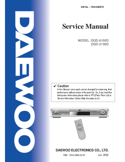
                              S/M No. : VD6100NET0


        Service Manual
                           MODEL :DQD-6100D
                                  DQD-2100D


 Caution
 : In this Manual, some parts can be changed for improving, their
   performance without notice in the parts list. So, if you need the
   latest parts information,please refer to PPL(Parts Price List) in
   Service Information Center (http://svc.dwe.co.kr).


 DAEWOO ELECTRONICS CO., LTD.
         http : //svc.dwe.co.kr                   Jun. 2002
  CONTENTS

EXTERNAL VIEWS .........................................................................................................2
   1. FRONT VIEWS ........................................................................................................................ 2

   2. REAR VIEWS............................................................................................................................2

SPECIFICATIONS ...........................................................................................................3
CIRCUIT DIAGRAM....................................................................................................................4
CIRCUIT OPERATIONAL DESCRIPTION ...............................................................................13
TROUBLE SHOOTING ..............................................................................................................26
WAVEFORMS............................................................................................................................36
COMPONENTS LOCATION GUIDE ON PCB BOTTOM VIEW ............................................45
DISASSEMBLY .........................................................................................................................47
ELECTRICAL PARTSLIST.........................................................................................................51


                                                                         1
   EXTERNAL VIEWS

1. FORNT VIEWS
   1)DQD-2100D


  2) DQD-6100D


2. REAR VIEWS
  1) DQD-2100D

                                                              AUDIO OUT (2 CH)VIDEO OUT


                    DIGITAL AUDIO OUT


                                                                                           EURO AV


  2) DQD-6100D

                                         AUDIO OUT (5.1 CH)    AUDIO OUT (2 CH)VIDEO OUT


                     DIGITAL AUDIO OUT


                                                                                           EURO AV


                                                          2
       SPECIFICATIONS

1. Prodcut features
-   Over 500 resolution of horizontal frequency
-   Disc playback of DVD, VCD, CD, CD-R, CR-RW
-   Dolby Digital decoding
-   5.1ch Analog signal output(6100, 6101)
-   DTS output
-   Screen zoom function
-   Special playback function(slow playback/fast playback)
-   Component output(Y, Cr, Cb)

2. Specifications

        Basic spec            orizontal frequency             over 500 resolution
                              available disc                  DVD, CD, VCD, CD-R, CD-RW, DVD-R

        Audio                 Dolby Digital                   Analog 5.1ch output and digital output
                              DTS                             Digital output
        Convenience           Screen zoom function            OK
                              Volume control function         OK
                              Special playback function       OK
                              MP3 playback function           OK

        Connecting terminal   Video terminal                  Composite terminal : 2 unit
                                                              Component terminal : 1 unit
                                                              S-VHS terminal : 1 unit

                              Audio terminal                  2ch terminal : 2 unit
                                                              5.1ch terminal : 1 unit
                                                              Optical terminal : 1 unit
                                                              Coaxial terminal : 1 unit

          Size                                                420x65x250 (WxHxD) Module : mm


                                                          3
  CIRCUIT DIAGRAM

POWER SUPPLY SCHEMATIC DIAGRAM(DQD-6100,220V)


                                                4
            CIRCUIT DIAGRAM


VIDEO


        5
CIRCUIT DIAGRAM


AUDIO


                  6
CIRCUIT DIAGRAM


VFD/JOG


                  7
          CIRCUIT DIAGRAM


ETC


      8
CIRCUIT DIAGRAM


VCR_INT(DVD)


                  9
                  CIRCUIT DIAGRAM


ATAPI(DVD)


             10
CIRCUIT DIAGRAM


CPU-ZR36703(DVD)


                   11
                    CIRCUIT DIAGRAM


MPEG DECODER


               12
CIRCUIT OPERATIONAL DESCRIPTION

POWER SECTION

 1. POWER SUPPLY OPERATION
    1) AC input and EMI FILTER
       AC inlet consists of Line Filter, X-Cap, Y-Cap, Varister. Line Filter(L801, L802), X-Cap(C803,
       C888), Y-Cap(C801) belong to EMI Filter section. They decrease noise to get into and out of AC
       Line.


                                Picture 1. [AC Input section]

   2) Primary rectification and smoothing circuit
      AC voltage passed through AC lnlet is rectified to Brige Rectification Diode D801 and changes to
      DC voltage. After that it smooths the Smoothing Condenser C806.
      When C806 is charged at first, Resistor R802 intercepts voltage current and protects D801, F801.
      Start Resistor R803, R804 supply Control IC VCC terminal with rectified DC voltage.


                         Picture 2 [Rectification, smoothing and starting circuit]


                                                  13
CIRCUIT OPERATIONAL DESCRIPTION


3) Sunbber circuit
 Sunbber circuit protects speedy voltage rising between Collector and Emitter when Main Switching TR is
 turned off. So Collector and Emitter voltage enter into safety operation and noise is decreased. When TR
 is turnd off, because high reverse voltage is generated between Collector and Emitter, it is rectified to
 D802, smoothed to C807 and consumed to R809. C808 is Speed-Up Capacitor.


                                      Picture 3 [Sunbber circuit]
4) Switching and Control Drive Circuit
   When Base of TR is charged through starting part, TR is turned on. So voltage is added to primary
   winding of transformer and genertaed at Base Drive. Because this voltage becomes to Positive Feedback
   voltage, TR is turned on again and Primary Winding of Trans is charged with electricity .


                                        Picture 4 [Drive Circuit]


                                                 14
                                                                         CIRCUIT OPERATIONAL DESCRIPTION


5) Costant-voltage Circuit
   This circuit maintains constant voltage. When voltage is lower or higher than reference voltage(2.5V) of
   IC801 pin1, this circuit compensates for a loss. Base voltage of Switching TR is controlled and final
   voltage is regulated by increasing or decreasing Internal Diode Current of IC801.


                                   Picture 5 [Costant-voltage Circuit]


   6) Secondary rectification circuit
      This circuit generates DC voltage needed to each terminal. It is rectified half-wave by D821, passes
      through Electrolytic Condenser C825 and generates the rectified DC voltage. DC voltage passes
      through L821, C822 and is removed of Ripple and Noise. The other terminal operation is same like
      this.


                                    Picture 6 [Secondary rectification circuit]


                                                     15
  CIRCUIT OPERATIONAL DESCRIPTION


7) Output terminal
   When power is turned off at power applied status, +3.3V is applied to Q822 Base terminal and Q824
   MOS FET outputs MVCC(+5V) to Drain terminal. When power is turned on, low signal(0V) is
   applied to Q822 Base terminal. At this time, Q824 MOS FET outputs MVCC(+5V) to Drain terminal
   and +5V to Source terminal. Q823 funcionates in same process and outputs +12M(Ever +12V) and
   +12V.


                                              Picture 7 [ Output terminal]

    2. POWER SUPPLY BLOCK DIAGRAM

                             Primary
                    NOISE                                                    Secondery
                             rectification
                    FILTER                                                   rectification
                             voltage
                                                                             voltage


                                                Starting
                                                Part       SUNBBER


                              Control Drive                Switching
                              Circuit


                                                                                             Costant-voltage
                                                                                             Control Drive
                                                                                             Circuit


                                                                       16
                                                                                                                                                                                             CIRCUIT OPERATIONAL DESCRIPTION


FRONT SECTION

1. VFD DRIVER
   1) Overview
     IC710 implements following functions by serial communication with MICOM depending on the software.
      * CMOS Technology
      * Internal Pull-Low Resistance
      * 4-step Dimming circuitry
      * Output from 8 to 18 Segment
      * Output from 7 to 10 Grid
      * Built-in Noise filter in Serial clock and serial Input Pins with 2MHz sampling
      * 8-bit x 6 channels Analog-to-Digital Converter with +-3LSB Accuracy
   2) Input/output port description
      * Input: It receives FPSEL, FPCLK and FPDOUT input from MICOM and KEY input by voltage Level.
      * Output: It outputs FPDIN with MICOM and operates FLD.
   3) Internal BLOCK DIAGRAM
                                                   GR10/SEG15


                                                                                            GR13/SEG12


                                                                                                                           GR15/SEG10
                                                                              GR12/SEC13
                                                                GR11/SEG14


                                                                                                          GR14/SEG11
                           GR8/SEG17
                                       GR9/SEG16


                                                                                                                                            GR16/SEG9
                                                                                                                                                            GR17/SEG8

                                                                                                                                                                        SEG7

                                                                                                                                                                               SEG6
                                                                                                                                                                                      SEG5
                                                                                                                                                                                              SEG4

                                                                                                                                                                                                      SEG3

                                                                                                                                                                                                              SEG2

                                                                                                                                                                                                                      SEG1
                                                                                                                                                                                                                              SEG0

                                                                                                                                                                                                                                       VCC
                             26          27 28 29                             30 31 32 33 34 35 36 37 38                                                                                     39 40 41 42 43                            44


          GR7/P7   25
          GR6/P6   24
          GR5/P5   23
          GR4/P4   22                                                                                                                       MODE                                      DISPLAY CONTROL
                                                                                                                                            REGISTER                                  CIRCUIT
          GR3/P3   21
          GR2/P2   20
                                                                                                                       TRANSFER                                                                      DISPLAY
          GR1/P1                                                                                                       COUNTER                                                                       MEMORY
                   19
          GR0/P0   18

          VEE      17
                                                                                                                                                                         BIYE END
                                                                             COMMAND ANALYTIC
          VEE      16                                                        CIRCUIT
                                                                                                                                                                                                       SERIAL
          SCLK     15    NOISE FILTER
                                                                                                                                                                                                       I/O
          SOUT     14
          SIN      13    NOISE FILTER
          CS
                   12    NOISE FILTER

                                                                                                                                                                        TRIGGER
                                                                                           SELECTOR/A.D                                                                                                       OSCILLATION
                                                                                           CONTROL CIRCUIT                                                                              A.D                   CIRCUIT


                                                                             11 10                       9             8                7               6                                             5         4      3       2         1
                                                                             AN0
                                                                                           AN1

                                                                                                         AN2

                                                                                                                       AN3

                                                                                                                                        AN4
                                                                                                                                                        AN5


                                                                                                                                                                                                      RESET

                                                                                                                                                                                                               OSC1


                                                                                                                                                                                                                                OSC2

                                                                                                                                                                                                                                            VCC
                                                                                                                                                                                                                        VSS


                                                                                                                                17
  CIRCUIT OPERATIONAL DESCRIPTION


2. Front Part Operational Description
    1) KEY SCAN & FLD Driver Interface


  2) Operation Description
  * If user presses KEY while IC500(ZR36705) implements KEY SCAN using VFD DRIVER(PT6355), the
    KEY input DATA go to IC500 by SERIAL Communication, then IC500 analyzes and processes the input
    DATA.
  * Implement the operation according to the input command and display the processing status on the VFD
    through PT6355
  3) Serial Communication Format


                                                 18
                                                                   CIRCUIT OPERATIONAL DESCRIPTION


AUDIO SECTION

1. 5.1 CH AUDIO DAC IC
   1) Overview
      24-BIT, 192-kHZ SAMPLING
      6-CHANNEL
      ENHANCED MULTILEVEL
      DELTA-SIGMA DIGITAL-TO-ANALOG CONVERTER
   2) Functions
     It, as a 5.1CH D/A converter IC, transforms Digital signals to Analog signals by receiving 3 CLOCK
     (System CLOCK, Shift CLOCK, Left and Right CLOCK) and 3 DATA from MPEG DECODER.
     Each 3 DATA associates to 2 CHANNELS.
     ->DATA1 : Main L.R CHANNEL
     ->DATA2 : Surround L.R CHANNEL
     ->DATA3 : Center, Woofer CHANNEL
      During Downmix, it receives only DATA1 from MPEG DECODER.
   cf) Downmix : Sound mixing method using 2 CH when the user doesn't have 6 CH amps or speakers but
       only have 2 CH.
   3) Internal Block Diagram


                                                  19
  CIRCUIT OPERATIONAL DESCRIPTION


2. 2CH AUDIO DAC IC(IC300) : PCM1748KE
   1) Overview
      24-BIT, 96-Khz sampling
      Enhanced multilevel
      Delta-sigma Digital-to-Analog Converter
   2) Functions
     It, as a 2CH D/A CONVERTER IC, receives 3 CLOCK and 1 DATA from MPEG DECODER and 3
     MODE control signal from MICOM, and then outputs Analog signal of L/R Channel.
   * MD : Mode Control Data Input
   * MC : Mode Control Clock Input
   * ML : Mode Control Latch Input
   * BCK : Audio Data Bit Clock Input
   * LRCK : L-Channel and R-Channel Audio Data Latch Enable Input
   * SCK : System Clock Input
   * DATA : Audio Data Digital Input
3) Internal Block Diagram


                                          20
                                                                  CIRCUIT OPERATIONAL DESCRIPTION


3. OP-AMP IC (IC303, IC304, IC305) : NJM4580M
   1) Overview
      Dual operational amplifier
   2) Functions
      It amplifies Analog audio signal from D/A Converter IC.
      Each associates to and amplifies 2 channels, and then outputs 5.1 Channel to JK300.
   cf) 2CH Audio DAC IC (IC300) model outputs 2 Channels to JK301 using only OP-AMP IC (IC 303).
   3) Internal Block Diagram


4. Hex Inverting Gates IC : (IC306)
   1) Overview
    It consists of 6 independent gates constructing Logic INVERT function
   2) Functions
    After Noise Filtering Digital audio signal from MPEG DECODER(IC405), it outputs the Digital audio
    signal to Coaxial(JK302).
   3) Internal Block Diagram


                                                 21
  CIRCUIT OPERATIONAL DESCRIPTION


5. General Audio Operation for 5.1CH
   1) Overview
     It receives CLOCK and DATA from MPEG DECODER(IC405) and transforms Digital signal to Analog
     signal at AUDIO D/A CONVERTER(IC350) then, amplifies Analog signal (IC303, IC304, IC305)and
     outputs to 5.1 CH Jack (JK300) and 2CH Jack (JK301).
    After Noise Filtering Digital signal from MPEG DECODER(IC405) at HEX Inverting Gates IC(IC306), it
    outputs Digital signal to Coaxial Jack (JK302).
   2) 5.1CH Audio Block Diagram
                                                              CH


                                                                     CH


                                                                          OUTPUT


                                                                          OUTPUT


6. General Audio Operation for 2CH
   1) Overview
     It receives CLOCK and DATA from MPEG DECODER(IC405) and MODE CONTROL signal from
     MICOM(IC500), and transforms Digital signal to Analog signal at AUDIO D/A
     CONVERTER(IC300) then, amplifies Analog signal (IC303) and outputs to 2CH Jack (JK301).
    After Noise Filtering Digital signal from MPEG DECODER(IC405) at HEX Inverting Gates
    IC(IC306), it outputs Digital signal.
   2) 2CH Audio Block Diagram


                                                 22
                                                                            CIRCUIT OPERATIONAL DESCRIPTION


MPEG B/D SECTION

1. Operational Description of MPEG B/D
   1) General Operation of B/D
   (1) Initial power supply operation
      When the power cord is plugged in, only EVER power is outputted to use minimum power supply such
      as u-COM and Flash Memory and MAIN power input is on standby status.
      If Power On Key is inputted, u-COM recognizes it and send Power On (L) signal to POWER, then the
      whole power is outputted from POWER and Set is in normal operation.
   (2) Function of MPEG B/D
     The general Set operation of Key operation and Power supply is controlled by u-COM, and DVD Format
     data Decoding and Video, Audio signal separation/output are executed in Loader.
     Here, Video output is in Analog and Audio output is in Digital Data Format to be inputted at Audio DAC.
     (See general block diagram below)


                                           Picture 1. [ General Block Diagram]

                                                      23
  CIRCUIT OPERATIONAL DESCRIPTION


2. MPEG Decoder : ZR36732(IC 405)
   1) Overview
    Because IC 405(ZR36732) includes Video Encoder function as well as MPEG Decoding function, it
    outputs Analog Video signal directly from IC. Output signal could be selected as either Composite/S-VHS
    composition or Composite/Component (Y, Cr, Cb) composition.
   2) Input/Output terminal
   * Input: It receives DVD MPEG Data inputted from MICOM at Loader.
   * Output: It outputs Analog signal of Composite, Component and S-VHS etc.
   3) Internal BLOCK DIAGRAM


                                 Picture 2. [MPEG Decoder Block Diagram]


                                                      24
                                                                                 CIRCUIT OPERATIONAL DESCRIPTION


3. U-COM: ZR36703(IC 500)
   1) Overview
     IC500 (ZR36703) controls the overall MPEG B/D, and receives DATA from Flash Memory and displays
     Logo screen, and controls MPEG Decoder to output Video/Audio signal by decoding MPEG format. It
     also controls OSD display such as Setup related to DVD.
   2) Input/Output terminal
     * Input:It receives DVD MPEG Data inputted from Loader, Data inputted from Memory and interface
             Data from IC (MPEG Decoder etc.).
     * Output: It outputs Control Data of each IC and Interface Data
   3) Internal BLOCK DIAGRAM


                                                            CPU


                                 DMA                                      BUS
                                 Controller                               Converter


                    INT 0 to     Interrupt                                                   BUS
                                                                             BUS
                    INT 5        Control                                                     Signal
                                                                             Controller
                                 Unit                                                        Data


                    AN 0 to    10-bit                                                        Memory
                    AN 3       A/D converter                                 DRAM
                                                                                             Data
                               (4 ch)                                        Controller


                   SIO-SI2       UART(3ch)                                   Port 0 to
                   SOO-SO2                                                   Port 3
                   SCO-SC2


                               A/V             A/V
                               Interface       Interface
                               Data            Port


                                                Picture 3. [CPU Block Diagram]
4. Other IC
   1) Flash Memory: SST 39VF400A (IC 502)
      It stores all programs for DVD operation and OSD language/Logo Screen Data, and transmits Data
      requested by CPU. The advantage of Flash Memory is that it can be updated without exchanging.
   2) SDRAM: GLT5160I16-7
     It executes video signal processing exchanging Data with MPEG Decoder. All the video signals
     transmitted from DVD go to SDRAM first, then through Video Encoder at MPEG Decoder and outputted
     finally as analog signals.


                                                           25
   TROUBLESHOOTING
1. POWER circuit
  Caution
 You must use insulated trance during the first part test of POWER circuit.


                           No POWER


                                                         NO
                   POWER cord/fuse is OK?
                                                                   Exchange POWER code/fuse

                       YES

                                                         NO
                  Voltage connected at D801?
                                                                       Check L801,L802

                       YES

                                                         NO
                  Voltage connected at L804?
                                                                         Check Q801

                       YES

                  Switching wave at T801 pin             NO
                           #6,7,8?                                  Check D803,D804,D805

                        YES

               D821, D822, D823, D824, D825,             NO
                   D826, D827 are OK?                               Exchange inferior ITEM

                       YES

                +5V obtained at IC802 base and           NO
                  +2.5V obtained at emitter?                          Check IC801, IC802

                        YES

                                                         NO
                +12V obtained at Q823 drain and +5V
                      obtained at Q824 drain?                          Check L812, L822


                +3.3V obtained at Q821, Q822 base when   NO
                          POWER OFF "H"?                              Check DVD PCB


              Check Q823, Q824, Q821, Q822 and
                     neighboring ITEM


                                                              26
                                                                                                          TROUBLESHOOTING


2. Front Circuits


                No VFD Letter Display or Broken
                            Letter


               -15V obtained at F(+), -19.5V at                NO
                           F(-)?                                              Check POWER circuit

                        YES

                 +5V obtained at IC710 pin #1,                 NO
                            #44?                                              Check POWER circuit

                        YES


               -24V obtained at IC710 pin #16,                 NO
                           #17?                                              Check POWER circuit

                        YES

               Input signal obtained at IC710 pin               NO
                                                                          Check communication line with
                         #12, #13, #15?
                                                                                   DVD B/D
                         YES

                                                               NO
                Pulse output at IC710 pin #14?
                                                                                 Check IC 710

                        YES

                  Oscillation at IC710 pin #2,                  NO
                              #4?                                                 Check IC 710

                         YES

              1.5V obtained at R760 when POWER switch is        NO
             pushed? 3V obtained at R761 when OPEN switch                        Check IC 710
              is pushed? 4V obtained at R762 when PAUSE
                            switch is pushed?
                        YES

                    Check communication line
                     between IC710 and VFD

             NO Problem                                     NO Problem
             Check wire connection between P710
                                                                            Check SW900, SW901
                          and P900


                                                                     27
TROUBLESHOOTING


3. AUDIO circuit
  Caution
 Before the AUDIO circuit test, check SETUP MENU setting first by remote controller.

A. Analog OUT
                    No AUDIO output from 5.1CH
                          JACK(JK300)


                          In case of 2CH setting                                  In case of 5.1CH setting

                             YES
                                                                            Is "Digital Output" item in Audio menu in
                   Speaker Downmix of SET UP Menu is set                   SETUP screen set properly to "Bitstream" or
                                                                                 "PCM" according to DVD title?
                             on Lt/Rt or Lo/Ro?                            Speaker Downmix of SET UP Menu is set on
                                                                           OFF/CENTER, BACK, SUBWOOFER ON?

                             YES                                                  Change SET UP menu setting
                                                            NO
                                                                   NO
                     CLOCK signal at P205 pin #6, 7, 8 and                 Check FFC CABLE connected to P205 and
                       DATA signal at pin #10, 11,13?                         MPEG Decoder IC pin #130-#141


                              YES
                                                                  NO
                   CLOCK signal at IC350 pin #18, 19, 20 and                        Check signal LINE
                       DATA signal at pin #1, 2, 3?

                             YES
                                                                   NO
                                                                             Check POWER circuit and +5V
                       +5V obtained at IC350 pin #15?
                                                                                      LINE

                              YES

                                                                   NO
                       AUDIO output wave at IC350 pin                                   Check IC350
                            #8,9,10,11,12,13?
                             YES
                                                                   NO
                                                                            Check POWER circuit and +12V LINE
                      +12V obtained at IC303,304,305 pin #8?

                             YES
                                                                   NO
                   AUDIO signal output at IC303,304,305 pin                       Check IC303,304,305
                                   #1,#7?

                            YES
                                                                 Problem
                        Check Q300,301,302,303,304,305                           Exchange inferior ITEM

             NO Problem

                        Check D308, 309, 310,311, 312,           Problem
                                                                                 Exchange inferior ITEM
                        313, 314, 315, 316, 317, 318, 319


                                                                   28
                                                                                                  TROUBLESHOOTING


 Caution
In case of COAXIAL and OPTICAL, check connection with receiver first before the circuit test.
B. Digital OUT
                     No AUDIO output from
                    COAXIAL JACK(JK302)

                        YES

                   RECEIVER is on COAXIAL            NO
                                                             Change RECEIVER setting
                          MODE?

                         YES


                 AUDIO DIGITAL signal at P205        NO   Check FFC CABLE connected to P205 and
                          pin #1?                               MPEG Decoder IC pin #133
                         YES


                                                     NO    Check POWER circuit and +5V
                  +5V obtained at IC306 pin #14?
                                                                    LINE

                         YES

                                                     NO
                 AUDIO DIGITAL signal at IC306 pin                   Check IC 306
                    #1,2,3,4,5,6,8,9,10,11,12,13?

                          YES                        NO Problem

                        Check D320, D321                       Check COAXIAL JACK


                     No AUDIO output from
                     OPTICAL JACK(JK303)

                         YES

                   Is RECEIVER on OPTICAL            NO
                                                             Change RECEIVER setting
                           MODE?

                         YES

                  AUDIO DIGITAL signal at P205       NO
                                                          Check FFC CABLE connected to P205 and
                           pin #1?                              MPEG Decoder IC pin #133

                         YES

                   +5V obtained at JK303 center      NO    Check POWER circuit and +5V
                              pin?                                  LINE

                         YES

                 Check OPTICAL JACK(JK303)


                                                             29
  TROUBLESHOOTING


4. VIDEO circuit
  Caution
 Before the VIDEO circuit test, check SETUP MENU setting first by remote controller.

                    No VIDEO output from JK301 yellow
                                  pin


                      TV setting on SETUP MENU is PAL           NO
                                                                          Change setting to PAL mode
                                     mode?

                              YES

                                                                NO        Check FFC CABLE connected to P205
                     Is there Video signal from P205 pin #20?
                                                                          and MPEG Decoder IC pin #100-#106

                              YES

                          Is there Video signal from            NO
                                                                               Check Q100, Q101
                             Q100,Q101 emitter ?

                              YES

                        Check D100,101,102,103


                      No Component Video output from
                                JK101


                                                                NO
                     TV setting on SETUP MENU is PAL mode?                    Change setting to PAL mode

                              YES

                     VIDEO output of SETUP MENU is              NO
                                                                           Change setting to Component
                           set on Component?

                               YES

                      Is there Video signal from P205 pin       NO        Check FFC CABLE connected to P205
                                  #17,18,19?                              and MPEG Decoder IC pin #100-#106
                               YES

                            Is there Video signal from          NO
                                                                             Check Q104,Q105,Q106
                            Q104,Q105,Q106 emitter ?

                              YES


                    Check D116,117,118,119,120,121


                                                                     30
                                                                                        TROUBLESHOOTING


      No S-Video output from
             JK102


 TV setting on SETUP MENU is PAL          NO
                                                       Change setting to PAL mode
                mode?

         YES

VIDEO output of SETUP MENU is set on S-   NO
                                                      Change setting to S-Video
                 Video?

         YES

Is there Video signal from P205 pin       NO        Check FFC CABLE connected to P205
              #18,19?                               and MPEG Decoder IC pin #100-#106
         YES

  Is there Video signal from Q102,Q103    NO
                                                          Check Q102,Q103
                 emitter ?

         YES


    Check D112,113,114,115


                                               31
 TROUBLESHOOTING


5. MPEG B/D


                             No LOGO display


                                                               NO    After checking Power_On_L Signal at
                               Is Power supplied?
                                                                           P505 pin#8, check CPU IC

                             YES

                     Does Oscillation Device oscillate?        NO
                                                                          Check OS500,OS401

                             YES

                   Is Digital Data transmitted from CPU        NO
                                                                       Check Flash Memory and CPU IC
                                 and Flash?
                             YES

                     Is Digital Data transmitted to SDRAM      NO
                                                                       Check MPEG Decoder IC
                           from MPEG Decoder IC?

                             YES


                            Check SDRAM IC


                         No Analog Audio output


                   Is Digital Data transmitted from CPU and    NO    Check Flash Memory and CPU
                                      Flash?                                      IC

                             YES

                   Is Digital Audio Data transmitted to MPEG   NO
                                                                           Check MPEG Decoder IC
                            Decoder IC pin #130-141?

                             YES

                     Is there Audio signal from P481 pin       NO    Check FFC CABLE connected
                                   #2-16?                                     to P481

                             YES

                            Check Analog B/D


                                                                32
                                                                               TROUBLESHOOTING


       No Digital Audio output


Is Digital Data transmitted from CPU and    NO    Check Flash Memory and CPU
                   Flash?                                      IC

          YES

Is Digital Audio Data transmitted to MPEG   NO
                                                      Check MPEG Decoder IC
           Decoder IC pin #133?

          YES

  Is there Audio signal from P481 pin       NO    Check FFC CABLE connected
                  #1?                                      to P481

          YES

         Check Analog B/D


                                             33
 TROUBLESHOOTING


6. SCART


                   No Audio with SCART Jack
                   (JK103)


                   Is there Audio signal in JK103     NO   Check JK103 and SCART
                            #1 and #3 pin?                 Cable.

                          YES

                   Check it with the same method of
                   2CH Setting of AUDIO circuit(1).


                     No Video with SCART Jack
                              (JK103)


                    Is "TV Type" item in Video menu   NO
                                                                 Set it to "PAL".
                     in SETUP screen set to "PAL"?

                           YES

                     Is there Video signal in P205    NO   Check FFC CABLE connecting
                                #20 pin?                     with P205 and check also
                                                           IC405 #103 pin in MPEG B/D.
                            YES

                       Is there Video signal in       NO
                                                                  Check Q107.
                            Q107 Emitter?

                           YES

                       Check D106 and D107.


                                                      34
                                                                                            TROUBLESHOOTING


 No conversion to MODE by pressing
  SCART button on remote control.


 Is there voltage change in Q111,
 Q112 Base like below each time
you press SCART button on remote
control (Mode Conversion)? (Only
       when H:3.3V, L:0V)

Terminal        Mode
                     AV AV Wide TV
Q111 Base(TV-CON)    H H         L        NO   Check CABLE connecting with P202 and check
Q112 Base(16/9-CON)  L H        H                 also IC500 #1 and #2 pin in MPEG B/D.
               YES

                                          NO
    Check Q110, Q111 and Q112.                        Exchange the bad Item.

 No Problem

 Is there voltage change to 12V, 6V and
   0V like below in JK013 #8 pin each
     time you press SCART button on
   remote control (Mode Conversion)?

Terminal        Mode
                       AV AV Wide TV Problem   Check R150, R151 and check
JK103 #8 pin           12V 6V     0V                also +12V LINE.


  No Problem

   Check JK103 and SCART
           Cable.


                                          35
      WAVEFORMS
1. MICOM/MPEG
   KDV-N TEST DVD VIDEO (TITLE1/CHAPTER4) Color Bar 100%


◦ Jabse Service Manual Search 2024 ◦ Jabse PravopisonTap.bg ◦ Other service manual resources online : FixyaeServiceinfo