Service Manuals, User Guides, Schematic Diagrams or docs for : Daewoo Plasma DP-42SM dae_dp42smlv_chas.sp115_plasma_438

<< Back | Home

Most service manuals and schematics are PDF files, so You will need Adobre Acrobat Reader to view : Acrobat Download Some of the files are DjVu format. Readers and resources available here : DjVu Resources
For the compressed files, most common are zip and rar. Please, extract files with Your favorite compression software ( WinZip, WinRAR ... ) before viewing. If a document has multiple parts, You should download all, before extracting.
Good luck. Repair on Your own risk. Make sure You know what You are doing.


Image preview - the first page of the document
dae_dp42smlv_chas.sp115_plasma_438


>> Download dae_dp42smlv_chas.sp115_plasma_438 documenatation <<

Text preview - extract from the document
                          S/M NO. : DSP115BEF2


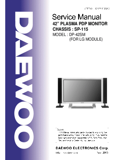
42" PLASMA PDP MONITOR
CHASSIS : SP-115
MODEL : DP-42SM
        (FOR LG MODULE)


 DAEWOO ELECTRONICS Corp.
 http : //svc.dwe.co.kr            Nov. 2003
                                        Contents
I. Parts with the exception of MODULE
1. Safety Precautions                                                         3
2. Product Specification
   2-1. SPECIFICATION                                                         4
   2-2. Available Input Signal                                                6
3. BLOCK DIAGRAM                                                              8
4. Description Of Each BLOCK
   4-1. A/V BLOCK                                                             9
      4-1-1. A/V BLOCK DIAGRAM                                                9
      4-1-2. VIDEO PCB                                                       10
      4-1-3. JACK PCB                                                        14
      4-1-4. KEY PCB                                                         15
      4-1-5. LED PCB                                                         15
   4-2. POWER PCB                                                            16
   4-3. BASIC CONGIFURATION                                                  17
5. SERVICE MODE
   5-1. Entering SERVICE MODE                                                18
   5-2. Default Values For SERVICE MODE Items                                18
   5-3. Description Of SERVICE MODE Items                                    19
6. Adjusting Method
   6-1. Adjusting WHITE BALANCE                                              23
   6-2. Adjusting POWER PCB                                                  23
7. SOFTWARE UPGRADE Method                                                   25
8. Main PCB Trouble Diagnosis                                                28
   8-1. VIDEO & JACK PCB Trouble Diagnosis                                   28
   8-2. POWER PCB Trouble Diagnosis                                          33
9. TROUBLE SHOOTING
   9-1. Facts You Must Know When Diagnosing And Repairing                    34
   9-2. Representative Symptoms When Each PCB Breaks Down                    34
   9-3. Trouble Diagnosis And Repairing Method For Representative Symptoms   35
10. ASSEMBLY LIST                                                            39
11. EXPLODED VIEW                                                            42


II. Parts of MODULE
1. Safety Precautions                                                        43
2. Formation and Specification of Module                                     46
3. Adjustment                                                                47
4. Trouble Shooting                                                          52
   4-1 Checking for No Picture                                               52
   4-2 Hitch Diagnosis Following Display Condition                           54

                                               -1-
      4-2-1. 4/7 or 3/7 of the screen doesn't be shown                                              54
      4-2-2. Screen doesn't be shown as Data COF                                                    54
      4-2-3. It is generated unusual pattern of Data COF IC unit                                    55
      4-2-4. Regular Stripe is generated about the quantity of one Data COF IC or more              56
      4-2-5. Screen doesn't be shown at all as scan COF                                             56
      4-2-6. Regular stripe is generated at regular internal on the whole screen                    57
      4-2-7. Data copy is generated to stripe direction                                             57
      4-2-8. One or more stripe is generated on the screen                                          58
      4-2-9. One or more horizontal line is generated on screen                                     58
      4-2-10. Lightness of screen is wholly darken though there is input-signal-pattern             58
      4-2-11. Different color is shown partially during full-white-screen or electric discharge is
              generated during full-black-screen                                                    59
      4-2-12. Full-white pattern it happened that the lightness of middle is darken while full-white
               pattern                                                                              59
      4-2-13. Some lightness of some color doesn't not generated well                               59
5. Block Diagram of Module                                                                          60


                                                   -2-
I. Parts with the exception of MODULE
1. Safety Precautions

1. Safety Precautions


(1) When moving or laying down a PDP Set, at least two people must work. Avoid any impact towards
    the PDP Set.


(2) Do not leave the broken PDP Set on for a long time. To prevent any further damages, after check the
    condition of the broken Set, make sure to turn the power (AC) off.


(3) When opening the BACK COVER, turn off the power (AC) to prevent electric shock. When a PDP
    is on, high voltage and high current exist inside the Set.


(4) When loosening screws, check the connecting position and type of the screw. Sort out the screws
    and store them separately. Because screws holding PCB are working as electric circuit
    GROUNDING, make sure to check if any screw is missing when assembling.

(5) If you open the BACK COVER, you will see a
   Panel Gas Exhaust Tube (Fig. 1). If this part is
   damaged, entire PDP PANEL must be replaced.
   Therefore, when working, be careful not to
   damage this part.


                                                                 Fig 1. Panel Gas Exhaust Tube


(6) A PDP Set contains a different kind of connector cables. When connecting or disconnecting
    connector cables, check the direction and position of the cable beforehand.


(7) When disconnecting connectors, unplug the connectors slowly with care. Especially when
    connecting/disconnecting FFC (film) cables or FPC cables, do not unplug the connectors too much
    instantaneously or strongly, and always handle the cables with care.


(8) Connectors are designed so that if the number of pins or the direction does not match, connectors
    will not fit. When having problem in plugging the connectors, make sure to check their kind,
    position, and direction.

                                                      -3-
2. Product Specification

2-1. SPECIFICATION
   ITEM                    SPECIFICATION                                         REMARK
1. GENERAL
   1-1. MODEL NO           DSP-4280LVS(G, W)
   1-2. CHASSIS NO         SP-115
   1-3. SCREEN SIZE        42 (16:9)
   1-4. COUNTRY            America
   1-5. RESOLUTION         852(H) X 480(V)
   1-6. REMOCON TYPE       R-V28A(E)
   1-7. SAFETY STANDARD    UL,C-UL,FCC(CLASS B)
2. MECHANICAL
   2-1. APPEARANCE
       1) WITHOUT STAND    WxHxD=1,044 x 631 x 82.8 mm
       2) WITH STAND       WxHxD=1,044 x 705.9 x 310 mm
       3) CARTON BOX       WxHxD=1,256 x 800 x 327 mm
   2-2. WEIGHT
       1) WITHOUT STAND    27.7 Kg
       2) WITH STAND       34.6 Kg
3. ELECTRICAL
   3-1. VIDEO INPUT        COMPOSITE (NTSC, PAL, SECAM, PAL-M/N, NTSC4.43)
                           & S-VHS (50/60Hz Y/C) 2 PORTS
  3-2. DTV/DVD INPUT       1080i, 720P, 480P , 480i
                           (Y, Pb/Cb, Pr/Cr, COMPONENT SIGNAL) 2 PORTS
  3-3. PC INPUT            VGA ~ UXGA (15 PIN D-SUB) 1 PORT
  3-4. SOUND INPUT         VIDEO 2 PORTS, DTV/DVD 2 PORTS,PC 1 PORT
  3-5. SPEAKER OUTPUT      8W(R) + 8W(L)
  3-6. POWER REQUIREMENT   AC 100V~240V, 50/60Hz
  3-7. POWER CONSUMPTION   320W
  3-8. RS-232 CONTROL      COMMUNICATION (EXTERNAL UPGRADE)
  3-9. FUNCTION
      1) SCREEN MODE       *PC: H/V SIZE AND POSITION ADJUSTMENT
                           *VIDEO : AUTO,16:9,PANORAMA,ENLARGE LB, ENLARGE LBS
                           *DTV/DVD : NOMAL,16:9
     2) ZOOM                20 STEP ZOOM
     3) OSD                11 LANGUAGES (ENGLISH,KOREAN,GERMAN,ITALIAN,
                           DUTCH,PORTUGUESE,SPANISH,MEXICAN,RUSSIAN,
                           CHINESE,FRANCH)
     4) OTHERS             STILL, SLEEP MODE , SOUND MODE


                                        -4-
                                                                        Product Specification


ITEM                           SPECIFICATION                                       REMARK
4. OPTICAL
    4-1. SCREEN SIZE           42 (106Cm) DIAGONAL
    4-2. ASPECT RATIO          16:9
    4-3. NUMBER OF PIXELS      852(H)X480(V)
    4-4. DISPLAY COLOR         16,700,000 COLOR( EACH 8BITS FOR RGB )
    4-5. CELL PITCH            1.08(H)X1.08(V)
    4-6. PEAK LUMINANCE        360cd/ (WITH FILTER GLASS)
    4-7. CONTRAST RATIO        1000:1
    4-8. VIEWING ANGLE         160(VERTICAL/HORIZONTAL)
5. USERCONTROL & ACCESSORIES
    5-1 CONTROL BUTTON(SET)    AC POWER BUTTON(PUSH-PULL S/W)
                               MENU, SELECT, UP, DOWN, LEFT, RIGHT(SOFT S/W)


  5-2. REMOTE CONTROL          POWER, INPUT SELECT, CONFIRM (or OK),
         ( R-28A(E) )          EXTENSION -, EXTENSION +, MENU, UP, DOWN,
                               VOLUME UP, VOLUME DOWN, SILENCE, PICTURE
                               MODE, PICTURE STILL, PICTURE SIZE, SOUND
                               MODE, TIMER SLEEP


  5-3. ACCESSORIES             REMOTE CONTROLLER,BATTERY,INSTRUCTION MANUAL,
                               A/V CABLE, PC CABLE, POWER CORD
                               OPTION : STAND WALL HANGER, SPEAKER R/L


                                           -5-
Product Specification


2-2. Available Input Signal
 (1) PC

 Resolution       H Freq. (KHz)    V Freq. (Hz)       Remark       Patt No.
  640x350             31.469           70.1            IBM           203
                      37.861           85.1           VESA            11
  640x400             24.823           56.4            NEC            15
                       30.48           60.0            PGA           871
                      31.469           70.1         IBM (DOS)        204
                      37.861           85.1           VESA            16
  640x480             31.469           59.9            DOS            17
                         35            66.7          Macintosh        18
                      37.861           72.8           VESA            19
                        37.5           75.0           VESA            20
                      39.375           75.0            IBM            21
                      43.269           85.0           VESA            22
  720x400              31.47           60.0            VGA           876
                      31.469           70.1            IBM            13
                      37.927           85.1           VESA            14
  720X480              31.54           60.0            480P          953
  720X576              15.63           25.0            PAL           950
  800x600             35.156           56.3           VESA            23
                       35.16           57.2           VESA            24
                      37.879           60.3           VESA            24
                      48.077           72.2           VESA            25
                      46.875           75.0           VESA            26
                      53.674           85.1           VESA            27
  832x624             49.726           74.0          Macintosh        28
 1024x768         48.193(48.077)    59.3(59.8)    Macintosh(OAK)     29
                      48.363           60.0           VESA            30
                       53.95           66.1            XGA           890
                      56.476           70.1         HP&VESA           31
                      60.241        74.9(74.6)       Macintosh        32
                      60.023           75.0           VESA            33
                      68.677           85.0           VESA            34
                       80.66          100.0           Fujitsu        939
                       70.84           84.0            SUN           926
 1152X864                54            60.0            VAX           936
                      63.851           70.0           VESA            35
                        67.5           75.0           VESA            36
                      77.094           85.0           VESA            37
 1152x900             61.796           66.0            SUN            38
                      71.713           76.0            SUN            39
 1280X720                45            60.0            720P          954
 1280X960                60            60.0           VESA            40
                         75            75.0           VESA            41
                      85.938           85.0           VESA            42

                                       -6-
                                                 Product Specification


 Resolution     H Freq. (KHz)   V Freq. (Hz)     Remark        Patt No.
 1280X1024         46.433          43.4           VESA           205
                   63.981          60.0           VESA            44
                    70.66          66.5           VAX            937
                    74.88          70.0           NEC            921
                   78.125          72.0        HP & HITA         206
                   78.855          74.1        Sony & NEC         46
                   79.976          75.0           VESA            47
                    81.13          76.1           SUN            927
                   91.146          85.0           VESA            48
 1600X1200          62.5           48.0           VESA
                      75           60.0           VESA            50
                    81.25          65.0           VESA           862
                     87.5          70.0           VESA           863
                    93.75          75.0           VESA           864
                     100           80.0           VESA           865

(2) DTV
-1080i/ 60 Hz
-720P / 60 Hz
-480P / 60 Hz

(3) VIDEO
-PAL, PAL-M, PAL-N
-NTSC , NTSC4.43
- SECAM


                                    -7-
                                                                   DSP-4280LVS BLOCK DIAGRAM

                                             Y-SUB PCB                                                                                                                                                                                        Z-SUB PCB
                                                                                                                                                                                             P3


                           IC


                    P1
                          SCAN
                         DRIVER
                                                                                                                                                                                       P2


                                                                                    P5
                                                                              PWR
                                                                                                                                                                                                                                  P1
                                                                                                                                                                                                                                       PWR


                           IC


                    P2
                          SCAN
                                                                                                                                                                                                                                                                  P5


                         DRIVER
                                                                                                                                                                                                                                                                       3. BLOCK DIAGRAM


                                                                                                                                                                                       p6


                                                                                    P6
                                                                              PWR
                                                                                                                     VIDEO PCB
                                                                                                                                      P601               P602
                                                                                                                                     KEY PCB         LED PCB
                                                                                                                                  Crystal : 14.3 MHz


                           IC


                    P3
                                                                                                                                                                                       P7
                                                                                                                                            20 MHz                                                     POWER PCB


                          SCAN


      Y DRV UPPER
                                                                                             P604
                                                                                                                    FLASH


                         DRIVER
                                                                                                                                            24.57 MHz
                                                                                                                   MEMORY         PLL CLK : 128 MHz


                                  P3
                                                                                                                                             33.5 MHz


                           IC
                                                                                                                                      DEINTERLACER


                    P4
                          SCAN
                                                                                                                                       [DPTV-MVS]


                                                                                                                                                                                       P4


                         DRIVER
                                                                                                                    IMAGE
                                                                                                                  PROESSOR
                                                                                                                   [PW171]
                                                                                                                                                                                                                                                                  P4


                                                                                                                                          VIDEO
                                                                                                                                       PROCESSOR


-8-
                                                                                                                                        [SAA7118]


                                                                                             PA5
                                                                                                    PWR
                                                                                                                                                                                       P5
                                                                                                                     ADC              3D COMBFILTER


                           IC
                                                                                                                  [CXA3516]             [UPD64083]


                    P5
                          SCAN
                         DRIVER
                                                                                                    PWR
                                                                                             PA4
                                                                                                                                                                                        AC                                                       PWR


                                  P4
                                                                                                                              P502                                                      P1                                             P2         P3


                           IC


                    P6
                          SCAN
                         DRIVER
                                                PWR
                                                P2         P1
                                                                                              JACK PCB
                                                                                                                              PA502                                                                PA6   PWR
                                                                                                Crystal : 4 MHz

                                              P300        P101
                                                                                                                   DTV/DVD                                                  SOUND
                                                PWR                                                                SWITCH                   AV SWITCH                     PROESSOR            SOUND AMP
                                                                                                                                             [CXA2069]


                           IC
                                                                                                                  [CXA2151]                                                [MSP3420]


                    P7
                                                                                                                                                                                                                                                             LEDPCB


      Y DRV UPPER
                          SCAN
                         DRIVER
                                                                                    P31
                                                                                                                                                                                                                  AC SWITCH


                           IC


                    P8
                          SCAN
                                                Clock Oscillator : 100 MHz


                         DRIVER
                                                                                                                         CONTROLLER PCB                                                X-RIGHT PCB
                                                                                                                                                                                                                                       P3         P5
                                                                                                                                                                                                                                                 PWR
                                                                                                                                                                         P1
                                                                                                                                                                                       P1


                    KEY PCB
                                                                                                                                                                                       P2


                                                                                                                                                                         P800


                                         P113                                   P112                              P111                                      P110                                    P212            P211                        P210


                                       DATA DRIVERIC                         DATA DRIVERIC                 DATA DRIVERIC                                 DATA DRIVERIC                            DATA DRIVERIC   DATA DRIVERIC              DATA DRIVERIC


                                  DATA COF                              DATA COF                          DATA COF                                  DATA COF                                  DATA COF            DATA COF                   DATA COF
4. Description Of Each BLOCK

4-1. A/V BLOCK
   4-1-1. A/V BLOCK DIAGRAM


                                                                            8

                                                                                  7


                                                                                                                                  1


                                                                                                                                                                             1
                                                                                         6

                                                                                                5

                                                                                                        4

                                                                                                                3

                                                                                                                         2


                                                                                                                                                 5

                                                                                                                                                         4

                                                                                                                                                                3

                                                                                                                                                                        2
                                                                            GND

                                                                                  E33V

                                                                                         GND

                                                                                                DATA2

                                                                                                        DATA1

                                                                                                                COLUM3

                                                                                                                         COLUM2
                                                                                                                                  COLUM1


                                                                                                                                                 STB5V

                                                                                                                                                          GND

                                                                                                                                                                LED_P

                                                                                                                                                                        IR
                                                                                                                                                                             GND
                                                                                               P601                                                         P602
                             P603
                                         1      RA1-   GND
                                 2                     RA1+           DEN
                                                RB1-
                                                       RB+       S_RESET
                                                GND                                                                                                                                VVS
                                                       RC-
                                                RC+               V_MUTE
                                                RCLK1+ RCLK1-      DVS                   IC600                                                     IC406
                                                RD1+   RD1-
                                                       GND         DHS                   PW171                                                   DPTV-MVS                          VHS
                                                RD2-
                                                RA2+   RA2-
                                                RB2+   RB2-
      to                                        RC2-   GND                                                                        VPEN1
                                                RCLK2- RC2+
   DIGITAL                                      RD2-   RCLK2+                                                                                                    VPEN
                                                GND    RD2+
                                                                             GBLKSLP            GPEN            GSOG
                                                SDATA DISPEN
                                 39             SLE    SCLK                                                                                               DECOE
                                         40            GND                  GHSFOUT            GCOAST GREF


                                                        DCLKB                                                                                      IC401
                             PA5                                                                                                                  SAA7118
                                 5       STB5V

                                 4       GND
                                                        GCLK                       IC500
                                 3                                                                                                                                      CCOMB
                                                                                  CXA3516
   to PWR                        2       POWER_CLT
                                                                 GHS
                                                                                                                                                                             YCOMB
                                 1       LED_P

                                                          GVS
                             PA4                                                                                                                          IC400
                                 10      STB5V                                                                                                           u64083
                                 9       LED_P

                                 8       GND

                                 7       GND                                                                                               VIN
                                                                 G/Y_DTV


                                 6       P5V
                                                                 Y_DVD
                                                                 R/PR
                                                                 B/PB
                                                                 GND

                                                                 GND

                                                                 GND

                                                                 GND

                                                                 GND

                                                                 GND

                                                                 GND

                                                                 GND

                                                                 GND
                                                                 GND

                                                                 GND

                                                                 GND
                                                                 GPC
                                                                 HPC


                                                                 RPC
                                                                 VPC


                                                                 BPC


                                 5       GND
                                                                 CO
                                                                 CR


                                                                 YO
                                                                 CB


                                 4       GND
   to PWR
                                                                 MSP_RST
                                                                 S_MUTE


                                                                                                                                                                                                            to PWR
                                                                 FB_SC


                                 3
                                                                 G_SC


                                         P12V
                                                                 R_SC


                                                                 B_SC
                                                                 P12V
                                                                 P12V


                                                                 SEL1
                                                                 SEL2
                                                                 SEL3
                                                                 GND
                                                                 GND


                                                                 GND


                                                                 GND


                                                                 GND
                                                                 GND

                                                                 GND

                                                                 GND


                                                                 GND
                                                                 RXD
                                                                 SDA

                                                                 TXD
                                                                 SCL


                                                                 VIN


                                 2       P12V
                                                         !P502


                                         !NUL                    1                                                                         25
                                 1
                                                                 26                                                                        50


                                                                 26                                                                         50                                                 1   2     3   4

                                          !JACK                  1                                                                          25
                                                                                                                                                                                                   !PA6
                                           PCB                                      !PA502
                                                                                                                                            R_OUT                                    RIGHT
                                                                                                                                                     L_OUT                                                   LEFT


                                                                                                                                                                              IC702                     IC701
                                                   IC706                            IC704                                                    IC700                           TDA7480                   TDA7480
                                                  CXA2151                          CXA2069                                                  MSP3420


     1   2   3   4   5   6   7       8
                                                                                                                                                                                                   1    2    3      4   5   6
                         PA601
    KEY PCB
                                                                                                                                                                                         LED                     PA602


                                                                                                -9-
Description Of Each BLOCK


  4-1-2.VIDEO PCB
     - PROCESS Various Signal (PC, COMPONENT, COMPOSITE ) to produce 24BIT DIGITAL
       output
     (1) IC and TP
        (1) IC400(UPD64083)
        -Using 3D COMBFILTER to separate COMPOSITE signal to Brightness
         Signal(Y) and Color Signal(C)

      *TP ( Input : COLOR BAR PATTERN )
            A. YCOMP : Brightness Signal(Y)


        B. CCOMP : Color Signal (C)


      (2) IC401 (SAA7118E)
      -Receive NTSC, SECAM, PAL VIDEO by COMPOSITE(V) , S-VHS(Y.C)
      COMPONENT (Y Cb Cr) and process signal

      *TP
            A. DECOE : CHIP ENABLE part. When signal process is done by IC401, DC 3.3V is
                       measured.


                                          -10-
                                                              Description Of Each BLOCK


(3) IC406(DPTV-MVS)
   -A Scan Rate Converter which converts Interlace signal into Progressive signal

  *TP
        A. VVS : VERTICAL SYNC (output of DPTV-MVS)


  B. VHS : HORIZONTAL SYNC (output of DPTV-MVS)


  C. VCLK : CLOCK (output of DPTV-MVS)


                                            -11-
Description Of Each BLOCK


    (4) IC500(CXA3516R)
       -3-channel 8-bit 165MSPS A/D converter which process PC , DTV signal

      * TP
             A. GCOAST : COAST CONTOL Signal for PLL (input of CXA3516)


      B .GHS : HORIZONTAL SYNC for GRAPHIC (output of CXA3516)


      C. GCLK : CLOCK for GRAPHIC (output of CXA3516)


                                             -12-
                                                 Description Of Each BLOCK


  D. GFBK : SYNC for PLL


(5) IC600(PW171)
   - Image processor IC

  *TP
        A. DEN : DATA ENABLE (output of PW171)


  B. DHS : HORIZONTAL SYNC (output of PW171)


                                     -13-
Description Of Each BLOCK


       C.DVS : VERTICAL SYNC for DISPLAY (output of PW171)


       D. DCLKB : CLOCK for DISPLAY (output of PW171)


  4-1-3. JACK PCB
      - Separate and process various VIDEO and AUDIO signal
      (1) IC706 (VIDEO /SYNC SELECTOR)
             - This chooses Y Cb/Pb Cr/Pr or RGB signal to output Y Cb/Pb Cr/Pr, to separate SYNC,
              and to perform SYNC COUNTER.

      (2) IC704 (AUDIO/VIDEO SWITCH)
             - The IC perform AUDIO or VIDEO SWITCHING

      (3) IC700 (MULTI STANDARD SOUND PROCDSSOR)
             -AUDIO SINGNAL VOLUME control, EQUALIZER control


                                               -14-
                                                        Description Of Each BLOCK

  *TP
        R_OUT(L_OUT) : AUDIO SIGNAL that goes into MSP3420 before AUDIO
        PROCESSING
(4) IC701 .IC700 (TDA 7480)


  *TP
        A. RIGHT(LEFT) :AMP input signal before 30dB amplification


4-1-4.KEY PCB
   - Input PCB using KEY
4-1-5.LED PCB
   - PCB for REMOCON CONTROL


                                        -15-
Description Of Each BLOCK


    4-2. POWER PCB

    
       Nominal Input Voltage : AC100V to AC240V (Variation Range - AC85V to AC276V)
       Single-Phase full wave
       Regulation Method : Transistor Switching Method
       Input Frequency : 50~60Hz (Variation range 45Hz to 66Hz)
       Inrush Current : 50A zero-peak max at AC264V
       Output Voltage is as follows.

   No.    Output Nominal     Variable     Voltage      Nominal    Load current Ripple/Noise
          Name   Voltage      range      accuracy      current       range      (mVp-p)*2
                   (V)         (V)          *1           (A)          (A)
    1      Vsus    190       180-195         5V          1.3        0.1~1.3      1000/500
    2      Vadd     60        50-80          2V           1          0.1~1        250/500
    3       V1     5.1          -            5%          2.5         0.1~3         50/100
    4       V3      17          -            5%           1           0~1          50/100
         (SOUND)   -17          -            5%           1           0~1          50/100
    5       V4     5.0          -            5%          1.5        0.1~1.5       50/100
    6       V5      12          -            5%          0.6          0~1          50/100
    7      Vstb      5          -            5%          1.5         0~1.5        100/100


  Connector
       Connector number          P2                     P3                 P6
          Model name        GP390-10P-TS            1-1123723-8       GP390-04P-TS
             Maker            LG Cable                 AMP              LG Cable
       The number of pins        10                      8                  4
               1             Vsus 190V              Vsus 190V              G
               2             Vsus 190V              Vsus 190V              G
               3             Vsus 190V                  NC              V1 5.1V
               4                NC                       G              V1 5.1V
   Pin         5                 G                       G
 number        6                 G                   Vadd 60V
               7                 G                       G
               8                 G                    V1 5.1V
               9                NC
              10                NC


                                           -16-
                                                                     Description Of Each BLOCK


       Connector number              P4                    P5                      P7
          Model name             YMW025-10R            YMW025-05R              YMW025-04R
             Maker                YEONHO                YEONHO                  YEONHO
       The number of pins            10                     5                       4
               1                     NC              POWER (ON/OFF)             V3 -17V
               2                     NC                   NC                       G
               3                   V5 12V                 NC                       G
               4                     G                     G                     V3 17V
   Pin         5                     G                    Vstb
 number        6                   V4 5V
               7                     G
               8                     G
               9                     NC
              10                     NC

* P2 is connected to P5 of Y-SUS PCB.
  P3 is connected to P1 of Z-SUS PCB.
  P6 is connected to P6 of Y-SUS PCB.
  P4 is connected to PA4 of VIDEO PCB.
  P5 is connected to PA5 of VIDEO PCB.
  P7 is connected to PA6 of JACK PCB.

     4-3. Basic Configuration


       Applied Voltage level is specified at the time, when full white pattern displayed on panel.

                                                  -17-
5. SERVICE MODE

5-1. Entering SERVICE MODE


  Push UP           MUTE          DISPLAY         MUTE BUTTON of Remote Controller to enter
  SERVICE adjustment MODE.


5-2. Check initial data of Video PCB

  (1) Check initial data of User Menu
     1) Picture
     - Mode : Normal
           BRIGHTNESS : 35
           CONTRAST : 47
           COLOR : 32
           TINT : 0 (CENTER) * Not displayed when PAL or SECAM input
           SHARPNESS : 4
     - Color Temp. : Normal
     2) Sound
     - Balance : 0 (CENTER)
     - Spatial Effect : Off
     - Sound Mode : Normal
           120 Hz : 0 (CENTER)
           500 Hz : 0 (CENTER)
           1.5 KHz : 0 (CENTER)
           5 KHz : 0 (CENTER)
           10 KHz : 0 (CENTER)
     3) Screen Mode : Normal
     4) Utility
     - Background : Opaque
     - Language : English ( selected when Power ON by user just after manufacturing )
     - ISM
           Pixel Shift : Off
           Low Bright : Off
           Image Invert : Off
     5) Input
     - VIDEO 1


  (2) Check initial data of Service mode
     1) PW 171
     - Sub-Brightness : 28
     - Sub-Contrast : 40
     - Bias R : 64
     - Bias G : 64
     - Bias B : 64
     - Gain R : 64


                                                -18-
                                                                                SERVICE MODE


     - Gain G : 64
     - Gain B : 64

  2) SAA 7118
     - Sub BRT : 128
     - Sub CONT : 50
     - Sub CLR : 55
     - Sub TINT : 0
     - Sub SRP : 10

  3) DPTV
     - Sub BRT : 61
     - Sub CONT : 16
     - 50 : OFF

  4) CXA 3516
     - Sub CONT : 58
     - Cb OFFSET : 39
     - Cr OFFSET : 37
     - HYS    :3
     - THRSLD : 14

  5) MSP34X0
     - PRESCALE : 22

  6) MISC
     - AT PWR : OFF
     - JACK : MULTI
     - PXL SFT : OFF

  7) PANEL
     - ISM : OFF
     - BWINV : OFF
     - GAMMA : 2.1
     - BRIGHT : 100 %
     - SCROLL : OFF
     - P SAVE : 75 %
     - MOVING : AV
     - STILL : PC

5-3. Description of SERVICE MODE Items

  1) PW171 : It is a Image processor and used to adjust White balance.
     [Note] This article is for adjustment after replacement of VIDEO PCB. These values may vary
            from set to set. Therefore if these values are recorded before replacing VIDEO PCB, you do
            not need to adjust WHITE BALANCE additionally. The setup can be done using the
            recorded values.

                                                -19-
SERVICE MODE


   (1) SUB BRT : For BRIGHTNESS adjustment (fixed)
   (2) SUB CONT : For CONTRAST adjustment (fixed)
   (3) BIAS R : For R BIAS adjustment (Changeable)
   (4) BIAS G : For G BIAS adjustment (Changeable)
   (5) BIAS B : For B BIAS adjustment (fixed)
   (6) GAIN R : For R GAIN adjustment (Changeable)
   (7) GAIN G : For G GAIN adjustment (Changeable)
   (8) GAIN B : For B GAIN adjustment (fixed)

 2) SAA7118 : It is a VIDEO DECODER and used to adjust a picture quality for VIDEO/DVD(480i).
    [Note] This article is not for adjustment after replacement of VIDEO PCB. Therefore do not
           change initial values.

   (1) SUB BRT : For BRIGHTNESS adjustment (VIDEO/DVD) (fixed)
   (2) SUB CONT : For CONTRAST adjustment (VIDEO/DVD) (fixed)
   (3) SUB CLR : For COLOR adjustment (VIDEO) (fixed)
   (4) SUB TNT : For TINT adjustment (VIDEO) (fixed)
   (5) SUB SRP : For SHARPNESS adjustment (VIDEO) (fixed)

 3) DPTV : Be used to adjust DEINTERLACE performance.
    [Note] This article is not for adjustment after replacement of VIDEO PCB. Therefore do not
           change initial values.

   (1) SUB BRT : For BRIGHTNESS adjustment (VIDEO/DVD) (fixed)
   (2) SUB CONT : For CONTRAST adjustment (VIDEO/DVD) (fixed)
   (3) 50P : ON for 50Hz / OFF for 60Hz (fixed)

 4) CXA3516 : It is a DTV/PC PROCESSOR and used to adjust a picture quality for DTV/PC.
    [Note] This article is not for adjustment after replacement of VIDEO PCB. Therefore do not
           change initial values.

   (1) SUB CONT : For CONTRAST adjustment (fixed)
   (2) Cb OFFSET : For Cb Offset adjustment (fixed)
   (3) Cr OFFSET : For Cr Offset adjustment (fixed)
   (4) HYS : For Sync hysteresis adjustment (fixed)
   (5) THR SLP : For Sync threshold adjustment (fixed)

 5) MSP34X0
    [Note] This article is not for adjustment after replacement of VIDEO PCB. Therefore do not
           change initial values.

   (1) PRESCLE : Be used to adjust a Audio prescale.

 6) MISC

   (1) TST PTRN AT : Cycled patterns from R G        B WH every 1 minute automatically.

                                              -20-
                                                                              SERVICE MODE


   (2) TST PTRN MA : Cycled patterns from BK WH R G B by pressing volume up key
   (3) AT PWR : ON - Condition where turning AC power on, automatically turns the SET on.
       OFF - Condition where turning AC power on makes the Set STAND BY, and POWER of
              Remote-controller on turns the set on from STAND BY state.
   (4) JACK : Set up depending on input MODE of JACK BOARD
        - SCART(SKY) : MULTI + DVI + SCART (DSP-4222LVS)
        - MULTI : Used by DSP-4280 series, Multimedia monitor.
        - MONITOR : Used by DSP-4282 series, PC only monitor.
        - MONITOR+ : Used by DSP-4282 series with DSP-JU20 attached, PC only monitor with
                          External board connection.
        - VIDEO : Video only monitor
      [Note] Wrong setup causes displaying problem. So you must be careful when SETTING.
   (5) PXL SFT : To choose a picture auto shift mode to protect a PDP(Ghost fault) ON - Moving
       screen up, down left and right by some Pixels every 20 seconds.
       OFF - Fixing PIXEL position. No movement on screen.
      [Note] PIXEL SHIFT function is solution to characteristic phenomenon of PDP, so-called
                Image Sticking problem. Leave this function ON, when displaying many fixed screen
              like PC screen. When this function is ON the screen will move a little for every fixed
              interval but a human eye can not recognize it well.
7) INFOR
   (1) VER : MICOM VERSION
       (year 4 digits, month 2 digits, date 2 digits and time 4 digits : 200309222030 )

8) RESET
   (1) EDID SET
   [Note] Be used to set to write EDID data (After setting it is changed to EDID DONE ). Before
          setting EDID, you have to short jumpers of JP710. After setting, you must remove jumpers,
          and then, turn off and on main power. If EDID WRITING ERROR is displayed, Try
          again. But, in DEUK, you don t have to set EDID set (After removing jumpers, EDID
          DONE is changed to EDID SET).
   (2) LEVEL 1 : Be used to initialise all of the data including adjusted figures for W/B.
   (3) LEVEL 2 : Be used to initialise all of the data except adjusted figures for W/B
   (4) FACTORY : For User menu initialisation, is actaviated by choosing a language on AC ON
       mode. (Menu Display, VOL, OSD Background and Input mode (VIDEO 1) initialisation).
       (Should be selected on being dispatched)

9) PANEL
   (1) ISM : Used to minimize Image
             Sticking (ON/OFF).
       ON : When Still images or regular
            patterns have been displayed
            on screen for some times, the
            luminance of screen is going
            to decrease as below. (But,
            only when pattern area is over
            50% and it is lasting over 5
            minutes)

                                              -21-
SERVICE MODE


   (2) BWINV : Used to minimize Image Sticking                    Table          Gamma Contents
                  (ON/OFF)                                          1                  =2.2
   ON : Inverting the original images.(in Digital image             2                   =1
         data, 0       1 , 1     0 )                                3              =2.1 (default)
    * If Still images have been displayed for some                  4                  =2.4
      periods, this function can minimize Image sticking,
      by displaying it on BWINV mode for some times.
   (3) GAMMA : can choose one in 4 gamma tables
   (4) BRIGHT : Adjusting Peak Luminance
      1. 100% : Full Peak Luminance
      2. 63% : 63% of Peak luminance
      3. 40% : 40% of Peak luminance
        (* See the graph below)
      4. APL: Average Picture Level


   (5) SCROLL : Minimizing Image Sticking (ON/OFF) by Shifting whole screen BRIGHT :
                    Adjusting Peak Luminance. (same with PXL SFT function in 6.MISC)
                       ON : This function moves1~8 pixel with a regular rule, up, down, left, right every
                       10 sec
   (6) BRIGHT : Adjusting Peak Luminance
   (7) P SAVE : Controlling power consumption by changing Luminance level of whole screen.
      1. 100% : Peak Luminance & Maximum Power Consumption mode
      2. 87% : 87% mode
      3. 75% : 75% mode
      4. 50% : 50% mode
      5. linear : linear mode(Constant luminance without regard to APL)
      * WARNING!! The choice of these modes can cause difference of Power Consumption.
      * See the below


   (8) MOVING : Setting display mode of Input channel except PC input.
   (9) STILL : Setting display mode for PC input.

                                                 -22-
                                                                         6.Adjusting Method

6-1. Adjusting WHITE BALANCE
   1) Apply 5 Step Gray Scale pattern to
      Video input terminal
      (MIK 7253S PATTERN NO.9)


                                                           Fig. 2 5 Step Gray Scale Pattern
  2) Check initial data of User Menu ( refer to 5-2 )
  3) To enter Service mode, press button up > mute > recall > mute on the remote controller and
     select PW171, then check initial data of Service mode( refer to 5-2 ).
  4) Attach a sensor of White Balance Meter(CA-100) to 80% of white level on the screen.
  5) Adjust White Balance by varying Gain of R,G,
  * Gain of R, G, should be adjusted to DP+ 10 ,if beyond these then that is a specification fault
  * Coordinate of Color is x=0.270 + 0.005, y=0.290 + 0.005 and the Color Temperature is over 10,000-
    degree K.
  6) Attach a sensor of White Balance Meter to 40% of white level on the screen
  7) Adjust White Balance by varying the values of R,G,
  * Values of R,G, should be adjusted to DP + 5 ,if beyond these then that is a specification fault
  * Coordinate of Color is x=0.270 + 0.005, y=0.290 + 0.005.
  8) Repeat No 4) to No 7) until getting that Coordinate of Color is x=0.270, y=0.290, and then adjust
     Sub Contrast to over 150 Cd/m square after attaching a sensor of White Balance Meter to 100% of
     white level on the screen.
  9) To exit from Service mode, press Menu button on the remote controller.

6-2. POWER ADJUSTMENTS
   * Video pattern condition : 100 IRE Full White Pattern
   * POWER PCB Adjustments mean that you should set the following 2-type power voltages to the
     values which were already adjusted by PDP module (LG Module) maker. Therefore, if there are
     some problems in picture after adjusting, you should classify that PDP module as a fault and contact
     to PDP module maker.

  1. Vsus (SUSTAIN Voltage) : Discharge Sustain Voltage
      Measurement equipment : Digital Volt Meter ( DC Volt mode )
      Adjusting TP : TP204 (See Fig. 4)
      Adjusting Location : RV203 (See Fig. 4)
      Optimum Adjusting Voltage : Voltage which is written in Label which is at upper right side of
      PDP Module. (Typical Voltage : 190 V - Fig. 3)


                                                  -23-
Adjusting Method


                       Fig. 3 Power Connection and Voltage Adjustment Label
  2. Vadd (ADDRESS Voltage) : DATA Input Voltage
        Measurement equipment : Digital Volt Meter (DC Volt mode)
        Adjusting TP : TP206 (See Fig. 4)
        Adjusting Location : RV204 (See Fig. 4)
        Optimum Adjusting Voltage : Voltage which is written in Label which is at upper right side of
        PDP Module. (Typical Voltage : 65 V - Fig. 3)


                                   Fig. 4 Power Adjustment Points
                                                 -24-
                                               7.SOFTWARE UPGRADE Method

1. Connect the JACK PCB to the Video PCB.
2. Connect 9 PIN serial cable to the serial port of the computer.
3. Connect the opposite end of the serial cable to RS-232C port of Jack PCB.
4. Run Flashupgrader.exe in PC and then push Next(N) > button.


5. Select current Upgrade file
   - Click Browse button to select the file you want to upgrade.


                                                  -25-
SOFTWARE UPGRADE Method


  - Select the file (pwSDK.inf) you want to upgrade and Push Open(O) > button.


6. Select as above and push Next(N) > button.

7. Select Comm Port and Baud Rate and push Next(N) > button.


                                                -26-
                                                            SOFTWARE UPGRADE Method


8. Upgrade process will be displayed. Turn on the ac power and then upgrade program will initiate the
   download.


9. When all files upgrade are complete, a window (below) will be opened. Push Finish button to
   complete the process.


                                                -27-
  8. Main PCB Trouble Diagnosis

  [NOTE] See II. PARTS of MODULE of this service manual for the trouble diagnosises concerned
         to MODULE with exception of VIDEO, JACK and POWER parts.
8-1. VIDEO & JACK PCB Trouble Diagnosis
   1. Common checking process when No signal or No raster

                  Check start

                              Y


                                                                                                          N       1. Confirm AC connection
                                                      N                            Is there a weak                2. Confirm Power S/W ON
             Does "No signal" screen
                                                                                  discharge on the                3. Check other PCBs
                    appear?
                                                                                       screen?                       (Refer to II. Parts of Module)

                                                                                              Y
                              Y
                                                                                                          N
                                                                                   Is P604 correctly                     Check P31
                                          N       Check the connection of             connected?
               Is the signal input Jack
                correctly connected?              Jack(PDP or AV devide)

                                                                                              Y
                              Y
                                          N                                     Is DVS, DHS, DCLK of          N
                  Does input source                                                                                   Exchange Video PCB
                (AV device)operate?
                                                   Operate AV device             Video PCB normal?


                              Y                                                               Y
                                              N      Confirm input          1. Check other PCBs (CONTROLLER,
             Is input selection in used                                        Y/Z-SUS, CONNECTION...)
                                                      selection
                       mode?                                                2. Reassemble or change P31


                              Y
             Exchange Video or Jack PCB


  2. When No VIDEO (COMPOSITE, S-VIDEO, Y Cb Cr) signal on screen
     (1) Input PC or DTV signal and see if PC or DTV signals shown on screen.
         If no signal, check TP DCLK, DHS and DVS signal.
          If DCLK, DHS and DVS signal do not appear, VIDEO PCB has a trouble.
     (2) When Y Cb Cr input : Check 16th pin of P502.


                                          COMPOSITE Input : Check TP Vin.


                                                                     -28-
                                                              Main PCB Trouble Diagnosis


            S- VHS input : Check 24th pin of P502 (when COLOR BAR PATTERN).


                      If above signal do not appear, JACK PCB has a trouble.
  (3) TP DECOE Check
      If DECOE signal do not appear, JACK PCB has a trouble.
       (cf. When COMPOSITE NTSC 3.58MHz, check TP COMB. CCOMB as well)

  (4) Check TP VVS, VHS, VCLK and VPEN1
      If VVS, VHS, VCLK and VPEN1 signal do not appear, JACK PCB has a trouble.

3. When DTV (1080i, 720P, 480P) signal do not appear on screen
   (1) Input PC or VIDEO signal and see if PC or VIDEO signals shown on screen.
       If no signal, check TP DCLKB, DHS and DVS.
       If DCLKB, DHS and DVS signal do not appear, VIDEO PCB has a trouble.

  (2) Check P502 s 1st PIN(V SYNC) , 2nd PIN(H SYNC) check-


      If above signals do not appear, JACK PCB has a trouble.
  (3) Check TP GHS, GVS and GCLK.
      If GHS, GVS and GCLK signal do not appear, JACK PCB has a trouble.

                                             -29-
Main PCB Trouble Diagnosis

  4. When PC signal do not appear on screen
     (1) Input DTV or VIDEO signal and see if DTV or VIDEO signals shown on screen.
      -->If no signal, check TP DCLKB, DHS and DVS.
      -->If DCLKB, DHS and DVS signal do not appear, JACK PCB has a trouble.
     (2) Check 1st PIN (V SYNC), 2nd PIN (H SYNC) of P502 (when 800X600).


    --> If above signal do not appear, JACK PCB has a trouble.
    (3) Check TP GHS, GVS and GCLK.
    --> If GHS, GVS and GCLK signal do not appear, JACK PCB has a trouble.

  5. When No Sound


                                              -30-


◦ Jabse Service Manual Search 2024 ◦ Jabse PravopisonTap.bg ◦ Other service manual resources online : FixyaeServiceinfo