Service Manuals, User Guides, Schematic Diagrams or docs for : Fluke 5x-2 datasheets DN2540
<< Back | HomeMost service manuals and schematics are PDF files, so You will need Adobre Acrobat Reader to view : Acrobat Download Some of the files are DjVu format. Readers and resources available here : DjVu Resources
For the compressed files, most common are zip and rar. Please, extract files with Your favorite compression software ( WinZip, WinRAR ... ) before viewing. If a document has multiple parts, You should download all, before extracting.
Good luck. Repair on Your own risk. Make sure You know what You are doing.
Image preview - the first page of the document
>> Download DN2540 documenatation <<
Text preview - extract from the document
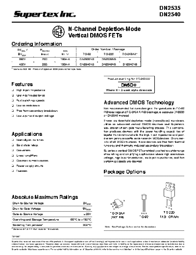
                                                                                                                                                                                DN2535
                                                                                                                                                                                DN2540

                                                                   N-Channel Depletion-Mode
                                                                   Vertical DMOS FETs
Ordering Information
      BVDSX /                    RDS(ON)                    IDSS                               Order Number / Package
      BVDGX                      (max)                     (min)                    TO-92                    TO-220                TO-243AA*
        350V                        25                    150mA                  DN2535N3                  DN2535N5                        --
        400V                        25                    150mA                  DN2540N3                  DN2540N5                 DN2540N8
* Same as SOT-89.        Product shipped on 2000 piece carrier tape reels.


                                                                                                                  Product marking for TO-243AA:

Features                                                                                                                          DN5D
 High input impedance                                                                                           Where  = 2-week alpha date code
 Low input capacitance
 Fast switching speeds
 Low on resistance
                                                                                                             Advanced DMOS Technology
                                                                                                             Not recommended for new designs. For products in TO-92
 Free from secondary breakdown                                                                               (N3) package and TO-243AA (N8) package, please use DN3535
 Low input and output leakage                                                                                or DN3545 instead.
                                                                                                             These low threshold depletion-mode (normally-on) transistors
                                                                                                             utilize an advanced vertical DMOS structure and Supertex's
                                                                                                             well-proven silicon-gate manufacturing process. This combina-
                                                                                                             tion produces devices with the power handling capabilities of
Applications                                                                                                 bipolar transistors and with the high input impedance and posi-
                                                                                                             tive temperature coefficient inherent in MOS devices. Character-
 Normally-on switches
                                                                                                             istic of all MOS structures, these devices are free from thermal
 Solid state relays                                                                                          runaway and thermally-induced secondary breakdown.
 Converters                                                                                                  Supertex's vertical DMOS FETs are ideally suited to a wide range
 Linear amplifiers                                                                                           of switching and amplifying applications where high breakdown
                                                                                                             voltage, high input impedance, low input capacitance, and fast
 Constant current sources                                                                                    switching speeds are desired.
 Power supply circuits
 Telecom
                                                                                                             Package Options


Absolute Maximum Ratings
                                                                                                                                     D
 Drain-to-Source Voltage                                                             BVDSX                           G
                                                                                                                         D                                                             G D
 Drain-to-Gate Voltage                                                              BVDGX                                 S                                                                S

 Gate-to-Source Voltage
◦ Jabse Service Manual Search 2024 ◦ Jabse Pravopis ◦ onTap.bg ◦ Other service manual resources online : Fixya ◦ eServiceinfo