Service Manuals, User Guides, Schematic Diagrams or docs for : Fluke 720A doc JW_EDN_p2
<< Back | HomeMost service manuals and schematics are PDF files, so You will need Adobre Acrobat Reader to view : Acrobat Download Some of the files are DjVu format. Readers and resources available here : DjVu Resources
For the compressed files, most common are zip and rar. Please, extract files with Your favorite compression software ( WinZip, WinRAR ... ) before viewing. If a document has multiple parts, You should download all, before extracting.
Good luck. Repair on Your own risk. Make sure You know what You are doing.
Image preview - the first page of the document
>> Download JW_EDN_p2 documenatation <<
Text preview - extract from the document
designfeature By Jim Williams, Linear Technology Corp
PART 2 OF THIS SERIES ON THE DESIGN OF A 20-BIT DAC DIS-
CUSSES THE ALL-IMPORTANT TECHNIQUES FOR TESTING THE
PERFORMANCE--LINEARITY, SETTLING TIME, AND NOISE--AT
SUCH MINUSCULE DATA LEVELS. SEE PART 3 IN THE NEXT ISSUE.
Measurement techniques
help hit the 1-ppm mark
true 20-bit DAC that fits on a circuit board
A and costs approximately $100 to build is a de-
sign milestone (see EDN, April 12, 2000, pg 95
or www.ednmag.com/ednmag/reg/2001/04122001/
R=100k
SEVEN-DECADE SWITCHED
WIPER POSITION PERMITS
SETTING TO 0.1-PPM LINEARITY
08ms743.htm). Claiming to achieve this level of per-
formance is one thing, but proving it with precise
(a)
measurements is another. The measurement tech-
10k 2k 400 80
niques are at times more exacting than the actual cir- INPUT
cuit's design. Part 2 of this series presents approaches
and circuits for measuring linearity, settling time,
and noise.
MEASURE LINEARITY TO 1 PPM
Of these three measurements, determining the
DAC's linearity requires the greatest effort. Verifying
1-ppm linearity of the DAC and the integral ADC
requires special considerations, and, interestingly,
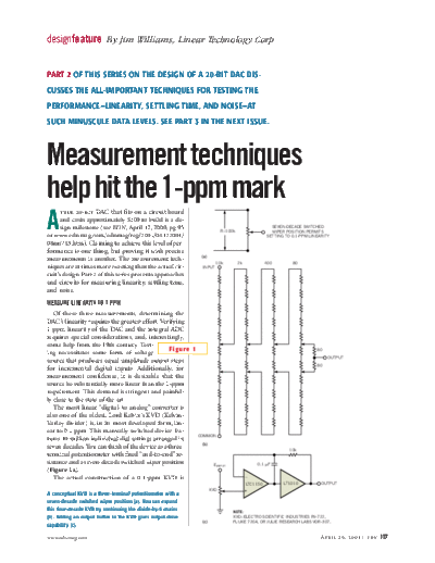
some help from the 19th century. Test-
Figure 1 80
ing necessitates some form of voltage
OUTPUT
source that produces equal-amplitude output steps
80
for incremental digital inputs. Additionally, for
measurement confidence, it is desirable that the
source be substantially more linear than the 1-ppm
requirement. This demand is stringent and painful-
ly close to the state of the art.
The most linear "digital-to-analog" converter is
also one of the oldest. Lord Kelvin's KVD (Kelvin-
Varley divider) is, in its most developed form, lin-
ear to 0.1 ppm. This manually switched device fea-
COMMON
tures 10 million individual dial settings arranged in
(b)
seven decades. You can think of the device as a three- 10k
terminal potentiometer with fixed "end-to-end" re-
sistance and a seven-decade switched wiper position EINPUT 0.1 F
(Figure 1a).
_
The actual construction of a 0.1-ppm KVD is
LTC1150 LT1010 OUTPUT
KVD +
A conceptual KVD is a three-terminal potentiometer with a
seven-decade switched wiper position (a). You can expand
this four-decade KVD by continuing the divide-by-5 chains NOTE:
(b). Adding an output buffer to the KVD gives output-drive KVD=ELECTRO SCIENTIFIC INDUSTRIES RV-722,
(c) FLUKE 720A, OR JULIE RESEARCH LABS VDR-307.
capability (c).
www.ednmag.com April 26, 2001 | edn 117
designfeature 20-bit DAC
more artistry and witchcraft second KVD to drive the main
than science. The market is rel- 10k KVD (Figure 3). Additionally,
5V
atively small, the vendors few, 0.1 F
an ensemble of three HP3458A
and the resultant price high. If _ voltmeters monitors the out-
$13,000 for a bunch of switches LTC1150 LT1010 OUTPUT put. The offset trim bleeds a
and resistors seems offensive, try KVD + small current into the main
building and certifying your RIN=100k KVD ground return, producing
WORST-CASE
own KVD. The KVD in Figure OUTPUT a few microvolts of offset-trim
1b has a 100-k input imped- RESISTANCE
30k
range. This range allows you to
ance. Thus, wiper's output re- functionally trim out all sources
sistance is high and varies with FLOATING, BATTERY- of zero error, such as amplifier
POWERED MICROVOLT
setting. As such, a very low bias- (a) NULL DETECTOR HP-419A offsets and parasitic thermo-
current follower is necessary to couple mismatches, permitting
unload the KVD without intro- REALISTIC a true zero-volt output when
ERROR WORST-CASE SELECTION ERROR IN
ducing significant error (Figure SOURCE SPEC TARGET PPM the main KVD setting is all ze-
1c). The LT1010 output buffer EOS 5 V 0.5 V 0.1 ros. Three voltmeters, which
allows for driving ca- E0S T 0.05 V/ C 0.05 V/ C 0.01/ C have a specification of less than
Figure 2
bles and loads and, IB 50 pA 10 pA 0.1 0.1-ppm nonlinearity on the
more subtly, maintains the am- CMRR 110 dB 140 dB 0.1 10V range, "vote" on the
plifier's high open-loop gain. FINITE GAIN 140 dB 140 dB 0.1 source's output. In other words,
The schematic in Figure 1c is (b) each voltmeter monitors the
deceptively simple. In practice, source's output. Then, you cor-
construction details are crucial. You can determine buffer error by measuring the I/O deviation with rect each reading for absolute
Parasitic thermocouples, or a floating microvolt null detector. This technique permits evaluation error and average the three cor-
namely the Seebeck effect; lay- of fixed and operating-point-induced errors (a). An error-budget rected readings to obtain the
out; grounding; shielding; analysis for the KVD buffer details the selection criteria (b). apparent linearity.
guarding; cable choice; and oth- The single-point-grounding
er issues affect achievable performance. or 5 V, and preferably at less than 0.5 scheme prevents the mixing of return
Part 3 discusses these issues in detail. In ppm. This test ensures that you account currents and the attendant errors. The
fact, as good as the chopper-stabilized for all error sources, particularly IB and shielded cables for connecting the KVDs
LTC1150 is with respect to drift, offset, CMRR, whose effects vary with operat- and voltmeters should have low-thermal-
bias current, and CMRR (common- ing point. Measured performance indi- activity specifications. Keithley type SC-
mode rejection ratio), selection is neces- cates that the sum of all errors called out 93 and Guildline #SCW are suitable.
sary if you seek sub-ppm nonlinearity in Figure 2b are well within desired lim- Crush-type copper lugs, as opposed to
performance. An error-budget analysis its. soldered types, provide lower parasitic-
details some of the selection criteria (Fig- thermocouple activity at KVD and DVM
ure 2). You can test the buffer with Fig- CIRCUIT CONSTRUCTION IS CRITICAL connection points. However, you must
ure 2a's circuit. As you run the KVD The detailed schematic of the sub- keep the lugs clean to prevent oxidation,
through its entire range, the floating null ppm-linearity voltage source includes thus avoiding excessive thermal voltages
detector must remain well within 1 ppm, offset trim, a stable voltage source, and a (see Part 3). A copper deoxidant (Caig
TABLE 1--HIGH-SENSITIVITY, LOW-NOISE AMPLIFIERS
Instrument Model Maximum Sensitivity
type Manufacturer number bandwidth or Gain Availability Comments
Differential amplifier Tektronix 1A7/1A7A 500 kHz/1 MHz 10 V/DIV Secondary market Requires 500 series mainframe,
settable bandstops
Differential amplifier Tektronix 7A22 1 MHz 10 V/DIV Secondary market Requires 7000 series mainframe,
settable bandstops
Differential amplifier Tektronix 5A22 1 MHz 10 V/DIV Secondary market Requires 5000 series mainframe,
settable bandstops
Differential amplifier Tektronix ADA-400A 1 MHz 10 V/DIV Current production Stand-alone with optional power
supply, settable bandstops
Differential amplifier Tektronix AM-502 1 MHz Gain=100,000 Secondary market Stand-alone with optional power
supply, settable bandstops
Differential amplifier Preamble 1822 10 MHz Gain=1000 Current production Stand-alone, settable bandstops
Differential amplifier Stanford Research SR-560 1 MHz Gain=50,000 Current production Stand-alone, settable bandstops,
Systems battery or line operation
118 edn | April 26, 2001 www.ednmag.com
designfeature 20-bit DAC
ADJUST FOR
STABLE 5.000000V AT A 10k
VOLTAGE
SOURCE
(LTZ1000A-
X 0.1 F 10k
BASED) _
LTC1150 LT1010 A X 0.1 F
10k X OUTPUT
KVD + _ 0.000000V
LTC1150 LT1010 TO
MAIN 10k 5.000000V
X +
KVD
+V
20k 2 F
OFFSET CASE
TRIM
2k
V
HP3458A
Figure 3 RWIRE
HP3458A
HP3458A
NOTES:
X=SOLDER-COPPER JUNCTION.
PLACE THE JUNCTIONS AND USE THE
NUMBER, AS NECESSARY.
2 F=POLYSTYRENE, COMPONENT RESEARCH CORP.
HIGH-QUALITY
GROUND
USE LOW-THERMAL, LOW-TRIBOELECTRIC SHIELDED
CABLE FOR KVD AND DIGITAL-VOLTMETER CONNECTIONS.
The complete sub-ppm-linearity voltage source includes offset trim, a stable voltage source, and a second KVD to drive the main KVD.
Labs "Deoxit" D100L) is effective for
maintaining such cleanliness. Low ther-
mal lugs and jacks, preterminated to ca-
bles, are also available (Hewlett-Packard
11053, 11174A) and convenient.
Thermal baffles that enclose the KVD
and DVM connections tend to thermal-
ly equilibrate their associated banana-
jack terminals, minimizing residual
parasitic-thermocouple activity.
Figure 4
Additionally, you should restrict
the number of connections in the signal
path. You also need to balance electrical
connections in the signal path against
each other such that the net signal-path
degradation due to thermocouples is
nominally equal to zero. When you in-
troduce a deliberate thermocouple, be
sure to match materials. Complying with
this guideline may necessitate a deliber-
ate introduction of solder-copper junc-
tions, marked "X" on Figure 3, to obtain
optimum differential cancellation (see
Part 3). Simply breaking the appropriate
wire or pc trace and soldering it facilitates
this cancellation. Ensure that the intro- In the sub-ppm-linearity voltage source, the LTZ1000A-based reference and buffers are at the
duced thermocouples temperature-track upper right. Offset trim is at the upper left, and reference and main KVDs are at the upper cen-
the junctions they are supposed to can- ter and center middle, respectively. Three HP3458 DVMs at the bottom monitor output. The
cel. You can usually ensure temperature computer in the left foreground aids linearity calculations.
120 edn | April 26, 2001 www.ednmag.com
designfeature 20-bit DAC
tracking by locating all junctions close to
each other.
The noise-filtering capacitor at the
main KVD is a low-leakage type; the
Figure 5
output buffer drives the capacitor's
metal to guard against surface leakage.
When studying this measurement ap-
proach, it is essential to differentiate be-
tween linearity and absolute accuracy.
This differentiation eliminates concerns
with absolute standards, permitting cer-
tain freedoms in the measurement
scheme. In particular, although Figure 3
uses single-point grounding, the circuit
does not use remote sensing. This choice
is deliberate, made to minimize the
number of potential error-causing par-
asitic thermocouples in the signal path.
Similarly, the design does not use a ra-
tiometric reference connection between
the KVD LTZ1000A voltage source and
the voltmeters for the same reason. In
theory, a ratiometric connection affords
lower drift. In practice, the resultant in-
troduced parasitic thermocouples obvi- In the reference-buffer box, the LTZ1000A reference circuitry is at the lower left, buffer amplifiers
ate the desired advantage. Additionally, are in the center, the capacitor-case bootstrap connection is center-right, and single-point-ground
the aggregate stability of the LTZ1000A "mecca" is at the upper left. The power supply at the top mounts outside of the box, minimizing
reference and the voltmeter references magnetic-field disturbances.
(also, incidentally, LTZ1000A based) is
comfortably inside 0.1 ppm for periods verifying KVD linearity by inter- uncertainty defined by the source and its
of 10 minutes, which is more than comparison with other KVDs and monitoring voltmeters is just 0.3 ppm.
enough time for a 10-point linearity by an independent calibration lab- This value is more than three times bet-
measurement. oratory, ter than the desired 1-ppm performance,
Figures 4 and 5 are photographs of the taking worst-case voltmeter ensem- promoting confidence in your measure-
voltage source and the reference-buffer- ble deviations over 0 to 5V every ments. A delightful activity, particularly
box internal construction. This KVD- 0.5V, and for those wholly unenthralled with Web
based, high-linearity voltage source has performing 100 runs (10 per day, surfing, is to spend hours "surfing the
been in use for years. The measurement once per hour). Kelvin." This activity consists of dialing
regime involves three steps: During this period, the total linearity various KVD settings and noting ADC
0 TO 5V
IN 0.5- V STEPS Figure 6
FROM BUFFERED KVD
5 pF
BIASED FROM
5V REFERENCE 5 pF
20k*
+ 5.1k 5 pF
20k*
LT1008 + 20 pF
FROM DAC 5.1k
_ LT1008 +
OUTPUT 5.1k
0 TO 5V 9k _ LT1008 +
5.1k
9k _ LT1008 OUTPUT
9k _
NOTES: 1k 5.1k
*VISHAY VHD-200 RATIO SET
1k
10-PPM MATCHING.
1k
1N4148.
909k 10 5.1k
1N5712.
CONNECT OUTPUT DIRECTLY
TO OSCILLOCSOPE. DO NOT 15V 15V
USE CABLE.
10k ZERO
TO SET ZERO, GROUND BOTH
INPUTS AND ADJUST ZERO
FOR VOUT LESS THAN 1 mV.
A clamped, distributed gain-of-2000 amplifier permits DAC settling-time measurements without saturation effects.
122 edn | April 26, 2001 www.ednmag.com
designfeature 20-bit DAC
agreement within 1 ppm. This astonish-
ingly nerdy behavior thrills certain types.
MEASURING DAC SETTLING TIME Figure 7
Measuring the 20-bit DAC's output
settling time is a challenging task. Al-
though the time scale involved is rela-
tively slow, the LSB step size of 5- V
presents problems. The issue reduces to
obtaining a great deal of gain without in-
ducing overdrive in the monitoring os-
cilloscope. Such overdrive will corrupt
the measurement, rendering displayed
results meaningless.
The input structure of Figure 6 resis-
tively balances the DAC output against
the precision variable reference supply,
such as in Figure 3, which is adjustable in
0.5- V steps. The circuit's remainder
constitutes a clamped, distributed gain-
of-2000 amplifier. Diode clamping at The settling-time amplifier's bandwidth is only 10 kHz, but its high gain of 2000 necessitates careful
each gain-stage input prevents saturation layout to avoid parasitic-feedback-induced oscillation. The input at lower left is fully shielded to
from occurring even with large DAC-ref- prevent radiative feedthrough to amplifier, and the enclosure shields the circuit from stray RF and
erence supply imbalances. The distrib- pickup.
uted gain allows a 10-kHz bandwidth
while maintaining clamping effective- sure to minimize effects of stray RF and similar results with standard mercury-
ness. The monitoring oscilloscope, oper- pickup. based reed relays. You test Figure 6's re-
ating at 5 or 10 mV/DIV (5 to 10 V at You can test the settling-time test cir- sponse by grounding one input and driv-
the DAC output) can readily discern 5- cuit by applying a test step that settles ing the other input with Figure 8a's pulse
V settling without incurring deleteri- much faster than the DAC. One method generator. The test circuit settles to with-
ous overdrive. is to use a mercury-wetted reed-relay- in 1 ppm ( 5 V) in 2 msec (Figure 8b).
Layout and construction of this circuit based pulse generator to supply the step This time is much faster than the DAC's
requires care. A linear layout minimizes (Figure 8a). The mercury-wetted reed re- settling time, lending confidence to the
parasitic feedback paths, preventing os- lay opens in 5 nsec, and the when the re- settling-time results of Part 1.
cillation (Figure 7). The construction lay opens, the circuit's output settles es-
fully shields the DAC input-step signal, sentially instantaneously relative to DAC MEASURING MICROVOLT NOISE LEVELS
preventing feedthrough to various sensi- speed and settling-time-amplifier band- Verifying DAC output noise requires
tive points within the amplifier. Finally, width. The relay in Figure 8a is com- a quiet, high-gain amplifier at the oscil-
the entire circuit sits in a shielded enclo- mercially available, but you can obtain loscope. Figure 9a shows one way to take
TEKTRONIX
Figure 8 067-0608-00
+V
MERCURY 25 mSEC
REED RELAY
5V 10 V/DIV
OUTPUT
FROM PULSE
PULSE 30 mSEC
IN
GENERATOR 50
TO DAC INPUT OF
SETTLE CIRCUIT
(GROUND SETTLE-CIRCUIT
REFERENCE INPUT)
(a) (b) 2 mSEC/DIV
A mercury wetted reed-relay-based pulser supplies a clean step to test the settling-time circuit (a), which responds to the test step with 2-msec settling
to ◦ Jabse Service Manual Search 2024 ◦ Jabse Pravopis ◦ onTap.bg ◦ Other service manual resources online : Fixya ◦ eServiceinfo