Service Manuals, User Guides, Schematic Diagrams or docs for : HP Publikacje 5966-1849E
<< Back | HomeMost service manuals and schematics are PDF files, so You will need Adobre Acrobat Reader to view : Acrobat Download Some of the files are DjVu format. Readers and resources available here : DjVu Resources
For the compressed files, most common are zip and rar. Please, extract files with Your favorite compression software ( WinZip, WinRAR ... ) before viewing. If a document has multiple parts, You should download all, before extracting.
Good luck. Repair on Your own risk. Make sure You know what You are doing.
Image preview - the first page of the document
>> Download 5966-1849E documenatation <<
Text preview - extract from the document
Agilent AN 1300-5
Electronic Characterization of IC Packages
Application Note
Agilent 4291B RF Impedance/Material Analyzer
1. Overview The leading implication is that the 3. The IC Package
This application note describes in impedance characteristics of the IC packages can vary in size, topology,
broad terms how to use the Agilent IC package leads will dramatically number of pins, substrate material,
Technologies 4291B RF Impedance/ contribute to reflections, overshoot, geometry, and lead length. Each has its
Material Analyzer in determining the undershoot, and crosstalk distortions own strengths and limitations. Within
impedance characteristics of IC pack- of the signal. This situation is com- all IC packages are lead frames, the
ages up to 1.8 GHz. This information is pounded by the rapidly shrinking conductors that connect the internal
useful for high speed digital designers, physical size of the IC packages leads, IC to a pc board. The lead frame is
component evaluation engineers, RF the processing of low level signals, imbedded on a rigid structure that
design engineers, IC package users in and the ever increasing pin density. becomes the IC package.
the analog or digital design environ-
ment, and for IC package manufac-
turers. This measurement solution
will accurately measure the imped-
ance, inductance, and capacitance
characteristics of IC package conduc-
tors and leads.
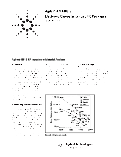
2. Packaging Affects Performance
The frequencies that ICs operate
at are growing higher. In computer
systems, clocks that now operate at
100 MHz will increase to 1 GHz by the
year 2000. Refer to Figure 2-1, Digital
Rate Trends. When chips run at high
frequencies (above 50 MHz) and the
signal edges consist of frequency
components that are much higher, the
lead conductors of IC packages that
link the chips to the circuit boards
start behaving like transmission lines.
The conductor will have inductance,
capacitance, and resistive elements. Figure 2-1. Digital rate trends
The lead frames are usually made up Self inductance (Lxx) A typical value can be up to hundreds
of copper alloy and have fine traces This is the number of magnetic field of milliohms, depending upon the
with different lengths and dimensions. lines around a single conductor (lead) type of lead material, lead length, and
These traces can have ends that ter- per amp of current flowing through surface area.
minate near the IC with a width of it. Typical values for a lead can range
0.10 mm. The intrinsic properties from 2 to 20 nH, depending upon the Interlead Capacitance (Cxo)
of the IC conductive and insulative length of the conductor and the phys- Lead capacitance is the amount
elements directly impact the extrinsic ical geometry of the lead. of electrical charge stored over the
characteristics (i.e., impedance) of an differential voltage between leads.
IC package. Although these character- Lead resistance (Rxx) Excessive lead capacitance can cause
istics can be estimated and modeled, This is an extrinsic property which crosstalk on adjacent channels. A typ-
modeling is not totally effective in relates the resistance of a structure to ical value can be about 1.8 pF per
describing the complete electrical the material and its geometry. It can be inch of conductor, depending upon the
performance of a specific IC package. derived from basic solid state princi- dielectric constant of the IC package,
Therefore, a measurement of the ples, and is related to the free charge lead length, lead cross-sectional area,
package must made to fully quantify carrier density and mean-free path. lead separation, and number of leads.
how an IC package will behave
under operating conditions.
4. Defining the Impedance
Test Parameters
The IC package impedance test
parameters that the 4291B can
measure are discussed below.
Impedance (Zo)
This is the total opposition the
conductor offers to the flow of an
alternating current. The impedance
represents the total effects of self-
inductance, mutual inductance, leads
resistance, interlead capacitance,
and interlead conductance. The IC
package in Figure 4-1 is an example
of a four element model.
Figure 4-1. IC package model
2
5. Choosing an Instrument operating away from a 50 test envi- The Agilent 4291B Impedance Analyzer
It not uncommon to characterize an ronment. Also, the swept data must is designed to address all of these
IC package from 1 MHz to 500 MHz, be mathematically converted to Z, L, issues. Refer to Figure 5-1, Measure-
1 GHz, or higher. Signal integrity about R, and C by using a computer. ment Accuracy. This chart shows the
the IC package is tested at the operat- typical 10% accuracy zones of a 4-ter-
ing frequency for analog design, like Fixtures and probes add inductive, minal pair impedance analyzer, a vec-
900 MHz for cellular RF applications. capacitive, and resistive parasitics tor network analyzer, and the 4291B
that add error to the measurement. over frequency and impedance.
Digital signal performance at nine The ability to compensate for these
times the fundamental is important parasitics is extremely important; The 4291B can also directly display
and needs to be characterized at the often the fixture parasitic values over- any two of the many impedance
odd-harmonic frequencies. whelm the conductor impedance values. parameters available, is specified to
Port extension is also very critical. operate from 0.1 to 50 k, has the
For example, a 50 MHz clock means IC packages do not easily mount onto distinctive capability of performing
the test frequencies start at 50 MHz for conventional 7 mm fixtures, so a cable compensation to remove probe para-
the fundamental and stop at 450 MHz must be connected from the measure- sitecs, and can easily extend the
for ninth harmonic characteristics. ment port to a fixture/probe. measurement port.
Measuring the impedance, inductance,
and capacitance characteristics of an From these measurement constraints, 6. The Probe
IC package can be quite frustrating. an instrument must have these mini- Using traditional handheld probes
Conventional impedance analyzers are mum capabilities: on today's high-density technologies
highly accurate but lack the needed can limit measurement accuracy and
high-end bandwidth. Vector network ◦ Jabse Service Manual Search 2024 ◦ Jabse Pravopis ◦ onTap.bg ◦ Other service manual resources online : Fixya ◦ eServiceinfo