Service Manuals, User Guides, Schematic Diagrams or docs for : HP Publikacje 5989-1618EN
<< Back | HomeMost service manuals and schematics are PDF files, so You will need Adobre Acrobat Reader to view : Acrobat Download Some of the files are DjVu format. Readers and resources available here : DjVu Resources
For the compressed files, most common are zip and rar. Please, extract files with Your favorite compression software ( WinZip, WinRAR ... ) before viewing. If a document has multiple parts, You should download all, before extracting.
Good luck. Repair on Your own risk. Make sure You know what You are doing.
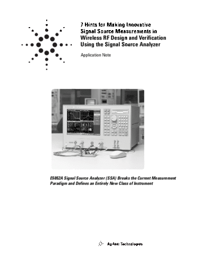
Image preview - the first page of the document

>> Download 5989-1618EN documenatation <<
Text preview - extract from the document
7 Hints for Making Innovative
Signal Source Measurements in
Wireless RF Design and Verification
Using the Signal Source Analyzer
Application Note
E5052A Signal Source Analyzer (SSA) Breaks the Current Measurement
Paradigm and Defines an Entirely New Class of Instrument
Importance of RF Design and Verification in Today's Wireless
Communication Systems
Market demands for today's Table 1. Examples of technical challenges to meet market demands
wireless communications Market demands Technical challenges
systems
To achieve higher data rates... Higher order and/or new
Today's wireless communications modulation/demodulation schemes
systems are required to simultane- (compressed decision point in the
ously provide better service quality constellation domain like 64 QAM/CDMA,
and lower costs. These expectations OFDM modulation, etc.)
are becoming increasingly difficult for
For more capacity and efficient spectrum Higher frequency operation
RF design engineers to accomplish
reuse... (system noise level increase, etc.)
due to multiple market demands -
such as higher data rates, more For multiple-mode operation... Hybrid system operation
capacity and efficient spectrum reuse, (multiple RF circuits)
multiple-mode operation (dual-mode, To achieve longer battery life... Low power consumption by RF module, IC
tri-mode), longer battery life, smaller To make the phone smaller... Additional integration (IC)
phone size, and a wide variety of (unknown spurious, noise, etc.)
software features such as i-mode.
To run a wide variety of software features... More powerful CPU/DSP processing
Importance of RF design and
Q
verification and today's
technical challenges
I
Although the baseband processing Effect of phase
and software implementations are noise on EVM
getting more important in today's
wireless communications systems,
RF design continues to be the key Effect of phase
area to meet or exceed customer noise on ACPR
demands and to differentiate your
products against competitors. This ACP
is because the RF design will
determine the most important basic
performance of your products, CH 1 CH2
like transmitter performance,
(modulation quality, adjacent Figure 1. Signal source effects in transmitter
channel power ratio (ACPR),
harmonics, spurious emission, etc.)
and receiver performance (sensitivity Receiver Receiver
noise distortion
and selectivity, etc.), as shown in
Figure 1 and 2. AM/PM
distortion
Phase noise & distortion
R Random noise
Threshold
To meet today's market demands, RF Bit error rate
Overload
(BER)
designers face many technical
challenges. Table 1 highlights the Phase noise
AM/AM AM/PM Delay distortion AM/AM
distortion distortion /ISI distortion
types of technical challenges that RF
Residual error floor
designers are required to overcome
in order to meet specific market Received signal level ( RSL)
demands. Phase noise
Interfering Receiver
signal LO
RF IF Downconverted
interfering
signal
+ LO = Downconverted
Wanted
signal wanted signal
Receiver IF BW
Figure 2. Signal source effects in receiver
2
Current Signal Source Design Process - Issues and Challenges
Signal source design process
System Circuit Circuit System
As shown in Figure 3, the typical simulation simulation verification verification
signal source design process is to
purchase or design a crystal
oscillator and voltage controlled
oscillator (VCO), then to design a Design or Purchase
loop filter for the PLL synthesizer in purchase crystal OSC
the circuit verification stage. The VCO
designers face issues and challenges
with each process, however VCO Crystal
sometimes it is difficult for the verification oscillator
designers to clearly identify or * Phase noise inspection
define the issue. * Freq, power,
* Close-to-carrier
DC current
phase noise
Lack of verification for crystal
oscillators, VCOs
Design loop filter
The high quality factor (Q) of the
crystal resonator and excellent long-
term stability are ideal for wireless
applications. If the crystal source is Synthesizer verification
incorrectly "assumed" to be good, * Phase noise
* Transients (freq/phase/power)
considerable effort may be expended
* Freq, power, spurious, harmonics
in vain trying to fix the wrong
components. In high-performance
wireless equipment with complex
modulations, achieving the lowest
possible phase noise begins with the Figure 3. Signal source design process
crystal source, so precise characteri-
zation is essential. However, it is
very hard to make such a low phase
noise measurement with the current
No optimum process for PLL New measurement challenges
phase noise test instruments. Thus, synthesizer cut & try for signal source design
the wireless equipment manufacturers Typical synthesized oscillators The recent signal sources require
do not inspect crystal oscillators combine a VCO with a phase locked new measurement challenges. For
and this is one of the biggest issues loop (PLL) IC, frequency reference instance, the phase noise perform-
when designing a RF circuit. (crystal /TCXO) and a loop filter. ance is getting lower and lower like
Furthermore, VCOs and synthesizers The loop filter design must integrate < ◦ Jabse Service Manual Search 2024 ◦ Jabse Pravopis ◦ onTap.bg ◦ Other service manual resources online : Fixya ◦ eServiceinfo