Service Manuals, User Guides, Schematic Diagrams or docs for : HP Publikacje HP-Bench-Briefs-1978-11-04
<< Back | HomeMost service manuals and schematics are PDF files, so You will need Adobre Acrobat Reader to view : Acrobat Download Some of the files are DjVu format. Readers and resources available here : DjVu Resources
For the compressed files, most common are zip and rar. Please, extract files with Your favorite compression software ( WinZip, WinRAR ... ) before viewing. If a document has multiple parts, You should download all, before extracting.
Good luck. Repair on Your own risk. Make sure You know what You are doing.
Image preview - the first page of the document
>> Download HP-Bench-Briefs-1978-11-04 documenatation <<
Text preview - extract from the document
6%
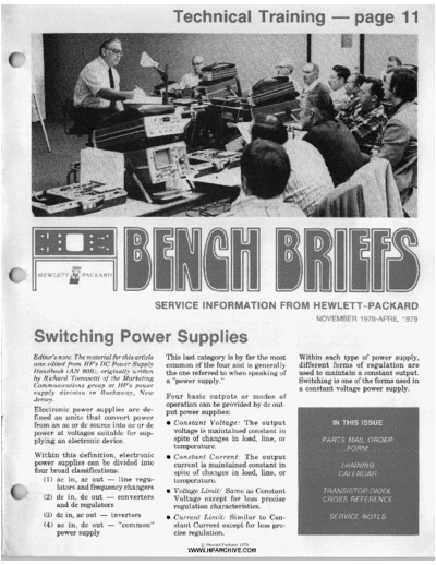
Technical Training - page. 11
a
SERVICE INFORMATION FROM HEWLETT-PACKARD
NOVEMBER 1978-APRIL 1979
Switching Power Supplies
Editor`s note: The material for this article This last category is by far the most Within each type of power supply,
was edited from H P s DC Power Supply common of the four and is generally different forms of regulation are
I ~ & o (AN ~o 9oB)j OrigkllY written the one referred to when speaking of used to maintain a constant output.
by Richard Tomasetti of the Marketing a ttpower supply.^^ Switching is one of the forms used in
Communications group at H P s power a constant voltage power supply.
supply division in Rockaway, New
r-----.
YtVSVJf.
Four basic outputs or modes of
operation can be provided by dc out-
Electronic power supplies are de- put power supplies:
fined as units that convert power
from an ac or dc source into ac or dc Constant Voltage: The output
power at voltages suitable for sup- voltage is maintained constant in
plying an electronic device. spite of changes in load, line, or
temperature.
Within this definition, electronic Constant Current: The output
power supplies can be divided into current is maintained constant in
four broad classifications: spite of changes in load, line, or
(1) ac in, ac out - line regu- temperature.
lators and frequency changers Voltuge Limit: Same as Constant
(2) dc in, dc out - converters Yoltage except for less precise
and dc regulators regulation characteristics.
(3) dc in, ac out - inverters Current Limit: Similar to Con-
(4) ac in, dc out - "common" stant Current except for less ipre-
power supply cise regulation.
* I
.- SWITCHING POWER SUPPLIES
operation at power line frequencies.
Typically, a switching supply is less that substantially
than one-third sim and weight of a 1 c o n b l output ripp
ching Regulated
2 &OWS a sohemdltic of one of
down through a power transformer, filter. Here the waveform is rectified
then rectified, which results in a and averaged to provide a dc output
lower voltage across its filter level that is proportional to the duty
(duty cycle) o the
f capacitor. of the waveform. Hence, in-
a d n g the ON timeas of the
tches i n c r e w the output volt-
age and vice-versa.
" b - w a d o r m of Fimre 2 Provide
a more detailed p i c k e of-circuit
Opera
tho*
sive, a fradion of the output voltage with a
some inherent operating charac- stable reference (EREF) produce
to
teristics that could limit its the VCONTROL level for the turn-on
Operating Advantages. Because effectiveness in certain applications. comparator. This device compares
One of these is that its transient re- the VCONTROL input with a triangu-
covery time (dynamic load regula- lar ramp waveform (A) occurring at
i slower than that of a series
s
ated supply. In a linear supply,
recovery time is limited only by the level, a turnsn signal (B) is
speeds of the semiconductors used generated. Notice that an increase
in the series regulator and control or derreaas in the VcoNTRoL volt-
age varies the width of the output I
by the indubce in the output fil- the switches.
1
ter. This may or lnay not be of sig-
e to the user, depending Steering logic within the modulator I
chip causes switching transistors ,
I
upon the specific application.
Q1 and Q2 to turn on alternately, so
Also, electromagnetic interference that each switch operates a t one-
(EMI) is a natural by-product of the half the ramp freguency or 20lrHz.
heat sinks. on-off switching. This interference
can be conducted to the load (result- Included, but not ehown, in the
weight reductions for ing in higher output ripple and modulator chip are additional cir-
supplies are a&ieved be- noise), it can be conduded back into cuits that establish a minimum
a t of their high switching rate.
~ ~ the ac line, and it can be radiated "dead-time" (off time) for the
The power transformer, inductors, into the surrounding atmosphere. switching transistors. Thia ensures
ter capacitors for 2OkHz that both switching tr-brs can-
n are much smaller and For this reason, all Hewlett- not conduct simultaneously during
than those required for Packard switching supplies have maximum duty cycle conditions.
WWW.HPARCHIVE.COM
ti
I
-
,.- . '
SWITCHING POWER SUPPLIES
.I 0 .-.
d the output lnductars and filter s a schematic of
capacitors. supply similar to
Figure 2 except for the addition of a
of surge protection must be provided Increasing the switching frequency, triac preregulator and associated
to limit line surge currents at however, would result in certain control circuit. The triac is a
turn-on. If not controlled, large benefits, including further size re- bidirectional device and is usually
surges could trip circuit breakers, ductions in the output magnetics connected in series with one side sf
weld switch contacts, or affect the and capacitors. Furthermore, tran- the input primary. Whenever a gat-
operation of other equipment can- sient recovery time could be de- ing pulse is received, the triae cozf-
nected to the same ac line. Protec- creased because a higher operating ducts current in a direction that is
tion is provided by a pair of ther- frequency would allow a propor- dependent on the polarity of the
mistors (Rto) in the input rectifier tional decrease in the output induct- voltage across it. The goal 3s to con-
circuit. With their high negative ance, which is the main constraintin trol the triac so that the bridge rec-
temperature coefficient of resist- recovery performance. tifier output (dc input to the
ance, the thermistors present a switches) is held relatively con-
relatively high resistance when cold stant. This is accomplished by a
(during the turn-on period) and a Unfortunately, higher frequency
operation has certain drawbacks. that issues a phase-
very low resistance after they pulse to the triac
heat up. One is that filter capacitors have an
Equivalent Series Resistance (ESR) once during each half-cycle of the
that limits their effectiveness at input ac. The control circuit com-
A shorting strap (Jl) permits the pares a ramp function to a rectsied
configuration of the input rectifier- high frequencies. Another disad-
vantage is that power losses in the ac sinewave to compute the proper
filter to be altered for different ac firing time for the triac.
inputs. For a 174-25OVac input, the switching transistors, inductors,
strap is removed and the circuit and rectifier diodes increase with Although the addition of the pre-
functions as a conventional full- frequency. To counteract these wgulator circuitry increases com-
wave bridge. For 87-127Vac inputs, effects, critical components such as plexity, it provides three important
the strap is installed and the input filter capacitors with low ESRs, fast benefits.
circuit becomes a voltage doubler. recovery diodes, and high-speed (1) By keeping the dc input to the
switching transistors are required. switches constant, it permits
Some of these components are al- the use of more readily avail-
ready available, others are not. able lower voltage switching
Switching Frequencies. Pre- Switching transistors are improv-
sently, 2OkHz is a popular repeti- transistors.
ing, but remain one of the major
tion rate for switching regulators problems at high frequencies. How- (2) The coarse preregulation it pro-
because it is a n effective com- ever, further improvements in vides allows the main regulator
promise with respect to size, cost, high-speed switching devices, such to achieve a finer regulation.
dissipation, and other factors. De- as the new power Field Effect Tran- (3) Through the use of slow-start
creasing the switching frequency sistors (FETE)would make high fre- circuits, the initial conduction of
would bring about the return of the quency operation and its associated the triac is controlled, providing
acoustical noise problems t h a t benefits a certainty for future an effective means of limiting
I plagued earlier switching supplies, switching supplies. input surge current.
4.
WWW.HPARCHIVE.COM
t
4
I i :1 11 SWITCHING POWER SUPPLIES
oftenIEgedin tudafs power supplies.
A is O the push-pull
f
version was used in
supplies shown in
Figures 2 and 3. Other variations of
Note that the freewheeling or catch diode) was
esmntially a s not requirsd in the two transistor formance applications. Push-pull
like the nutin regulator switches, regulators of Figures 2 and 3 be- circuib have the advantage d a rip
does not abaorb a large amount of cause of their full-wave rectifier ple frequency that is double that of
power. Hence, the addition af the configuration. the other two basic configurations
pmregdator does not significantly output ripple is
reduce the overall efficiency of this Another item not found in the previ-
SupplY.
Stngle Transistor Switching
Rectr;clafor
At lower output m e r levels, a o m -
trm-r mt& tieGamee
ii
The single hisistar
Fidfurs4is*dto
or f d w - , converter, It am 4
wive a dc input f o either one of
rm function because core saturation
two sources without a change in its often leads to the destruction of
ration. For ac-to-dc switching transistors. In the previ-
the regulator is con- ously described two transistor
..
push-pull ciraits, core saturation is
e&ier to avoid became ma@&nmg
t is applied %o core in both
the
directitma (Le., Mom saturatkoa,
t;hs txlmmt ia m w d ) . Nevp*@-
Like the previous switching ConfigurationB is a UBefUl alterna-
ea& 20kHz clock pulse and turned
off by the pulse-width modulator mediately following turn-on of the
at a time determined by output load switch. Although the ripple fre-
Conditions. quency is inherently lower, output
ripple amplitude ixin be eXff"ective1y
While the regulating transistor is contFolied by the choke in &e output
-
conducting, the half-wave rectifier filter. Two-transistor configurations
of forward converters alw exist
diode i forward biased and power is
t
s
to the output f l e and
itr
the load. When the regulator is
wherein both transistore are
switched simultaneously. They pro-
0
turned off, the "flywheel" diode con- vide the same output power as the
hd, * * gcurrentflowtothe single transistor versions, but the
load during the off period. A transistors need handle only half the
flywheel diode (sometimes called a peak voltage.
WWW. H PARCHIVE.COM
Configuration C is known as a
flyback, or ringing choke, converter
because energy is transferred from
primary to secondary when the
switches a m off (during flyback). In
the example, two transistors are
used and both are switched simulta-
neously. While the switches are on,
the output rectifier is reverse biased
and current in the primary induct-
ance rises i n a linear manner.
When the switches are turned off,
the collapsing magnetic field re-
verses the voltage across the pri-
mary, and the previously stored en-
ergy is transferred to the output fil-
ter and load. The two diodes in the
primary protect the transistorsh m
M w t i v e aurgea that owur st turn-
Off.
safe level.
WWW. H PARCHIVE.COM
SWITCHING POWER SUPPLIES
I1
Switching Power Supply Terminology
The following is a brief glossary of The terms %oise'' EMI and RFI are caused by charging of the input
terms encountered in dealing with sometimes used in the same context. capacitor, and limited primarily by
switching supplies. an input thermistor or preregulator.
ESR (Equivalent Series
Brown Out Rated Resistance) Input Voltage Range
The amount of resistance in series The range of line voltages for which
The ability of a power supply to with a n ideal (lossless) capacitor
maintain regulated output voltages the power supply meets its specifica-
which exactly duplicates the per- tions. The lowest line voltage is im-
in the event that the input line volt- formance of a real capacitor. In gen-
age should drop to a low or zero portant in defining the relative de-
eral, the lower the ESR, the better gree of brown-out protection.
level. the quality of the capacitor and the
more effective it is as a filtering
Current Foldback device. ESR is a prime determinant Isolation Voltage
of ripple in switching supplies. The maximum voltage by which any
An overload protection method
where output voltage and current part of the circuit can be operated
decrease simultaneously as the load Flyback away from chassis ground. Also the
resistance decreases below a preset maximum voltage between any out-
Precisely, it's the shorter of the two put and input terminal.
crassover point and begins to ap- time intervals comprising a saw-
proach a short circuit. Also known as tooth wave. In a switching power
output short circuit protection, this supply, the shorter interval is pro- Line Regulation
mechanism monitors the outpuk cur- duced when the transistors are See Source Effect.
rent and, if it exceeds a preset cross- switched off. This causes a rapidly
over value, turns down the regulator collapsing magnetic field in the
output. transformer which reverses the Line Frequency Regulation
voltage across the primary, transfer- The variation of an output voltage
ring a high energy to the output. due to a change in line input fre-
quency with all other factors held
constant. This effect is negligible in
Ground Loop switching and most linear supplies,
A feedback problem caused by two or but is very critical in ferroresonant
more circuits sharing a common supplies.
electrical line, usually a common
ground line. Voltages gradients in Load Effect Transient Recovery
this line caused by the first circuit Time
may be resistively, inductively, or Sometimes referred to as transient
capacitively coupled into the other recovery time or transient response
circuit via the common line. With time, it i ,loosely speaking, the time
s
reqtllred for the output voltage of a
reduced using single point ground- power supply to return to within a
ing near the supply. level approximating the normal dc
EMI (RFD output following a sudden change in
Electromagnetic interference (radio Hold-up Time load current. More exactly, Load
frequency interference) -unwanted Transient Recovery Time for a CV
high frequency energy caused The total time any output will supply is the time "X"required for
primarily by the switching compo- remain within its regulation band the output voltage to recover to, and
nents in the power supply. EMI can after line input voltage has suddenly stay within "Y"millivolts of the
be conducted through the input or dropped to zero or below rating. nominal output voltage following a
output lines or radiated through the Hold-up is measured at full load and "Z" amp step change in load current
unit's case. Conducted EM1 (RFI) nominal line conditions. - where:
can be reduced using proper filter-
ing, and radiated EMI (RFI) can be (1) "Y" specified separately for
is
reduced by judicious board layout Input Surge Current each model, but is generally of
and enclosing the supply in a metal The peak line current which flows the same order as the load
enclosure. during turn-on. Surge current is regulation specification.
WWW.HPARCHIVE.COM
-
SWITCHING POWER SUPPLIES 1 1: i 6 i ::: 1
11
m (2) T h e n o m i n r x l a u t p u t v o l ~ i s "wmb&` i u1BBd t rapidly place a
defiwrd 8e the dc level half-
way between the steady atate
s a
short circuit across tzle output ter-
m i n d s whenever the threshold volt-
output voltage before and age i exceeded.
s
after the imposed load
change.
PARD (Ripple and Noise) to a minimum, dissipative losses are
generally s a l
ml.
(3) "2" is the specified load cur- The term PARD is an acronym for
rent change, typically equal "periodic and random deviation" and
to the full load current rating replaces the former term ripple and Rise Time and F l Time
al
of the supply. noise. PARD is the residual ac com-
ponent that ie superimposed an the When applied to the switching tran-
dc output voltage or current of a sistor, that time in which-non-zem
power supply. It is measured over a currents and voltages result in high
specified bandwidth with all influ- peak pdwer dissipation. Carehl at-
ence and control quantities main- ion must be paid to reducing
tained constant. PARD is specified es, particularly when
inductive loads.
Rippls and Noise
PARD with an instrument that has See PARD.
insuflicient bandwidth may conceal
high frequency spikes that could be
detrimental to a load. Short Circuit Protection
See Current Foldback.
C OUTPUT OF POWER SUPPLY
SUPERIMPOSED PARD Source Effect (Line
Regulation)
Formerly known as line regulation,
source effect is the change in the
Overcurrent Limiting steady-state value of the dc output
voltage (of a CV supply) or current
A protection mechanism which lim- (of a CC supply) due to a specified
its the output current of a supply change in the source (ac line) volt-
without materially affecting the age, with all other influence quan-
output voltage. tities maintained constant. Source
effect is usually measured after a
Overshoot "complete" change in the ac line
voltage from low line to high line or
vice-versa.
The amount by which an output ex- Peak Charging
ceeds ita final value in a transient
response to a rapid change in load or A rise in voltage across a capacitor Switcher
input voltage. In power supply de- caused by the charging of the
sign this parameter is particularly capacitor to the peak rather than A common industry-wide name for a
important at turn-on. RMS value of the input voltage. This switching power supply.
generally occurs when a capacitor
has a high discharge resistance
Overvoltage Protection across it and large ripple or spikes on Temperature, Coefficient
A protection mechanism for the load its input line. In a switcher this effect The average percent change in out-
which reduces the output voltage to determines minimum load (dis- put voltage per degree change in
a very low value in the event that charge resistance) conditions on each temperature with load and input
the output !exceeds a certain output to maintain regulation. voltage held constant. The coeffi-
threshold voltage. In a switching. cient is usually derived from output
supply, the regurator is turned off 8
the threshold is exceeded. reducing:
post bwator voltage measurements taken at
room temperature (25◦ Jabse Service Manual Search 2024 ◦ Jabse Pravopis ◦ onTap.bg ◦ Other service manual resources online : Fixya ◦ eServiceinfo