Service Manuals, User Guides, Schematic Diagrams or docs for : HP Publikacje HP-Bench-Briefs-1982-07-10
<< Back | HomeMost service manuals and schematics are PDF files, so You will need Adobre Acrobat Reader to view : Acrobat Download Some of the files are DjVu format. Readers and resources available here : DjVu Resources
For the compressed files, most common are zip and rar. Please, extract files with Your favorite compression software ( WinZip, WinRAR ... ) before viewing. If a document has multiple parts, You should download all, before extracting.
Good luck. Repair on Your own risk. Make sure You know what You are doing.
Image preview - the first page of the document
>> Download HP-Bench-Briefs-1982-07-10 documenatation <<
Text preview - extract from the document
!
I
I
SERVICE IhlFQRMATlON FROM HEWLETT-PACKARD
I REFERENCE FILE COPY JULY-OCTOBER 1982
PLEASE DO NOT REMOVE grounded soldering iron and needle-
nose pliers (see Figures 3 and 4).
This method is very effective since
it minimizes the chance of over-
Jim Bechtold. Editor heating and damaging the PC board.
Introduction looks as though this person used a
100-watt soldering gun in the area
Since there are recognized proce- indicated by the arrow. Figure 2
dures for logical troubleshooting, shows a different repaired area with
there should also be recognized pro- good solder techniques; but then the
cedures for removing the defective person made the mistake of trying
components, installing new ones, to remove the flux with a sharp-
and in general, repairing defective pointed tool.
printed circuit (PC) boards. There
are accepted procedures, and this
article will describe some of Hewlett-
Packard's standards and methods for
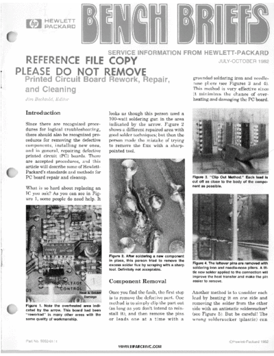
PC board repair and cleanup. Figure 3 "Clip Out Method." Each lead is
.
cut off as close to the body of the compo-
nent as possible.
What is so hard about replacing an
IC you ask? As you can see in Fig-
ure 1, some people do need help. It
Figure 2. After soldering a new component
in place, this person tried to remove the
excess solder flux by scraping with a sharp Figure 4. The leftover pins are removed with
tool. Definitely not acceptable. soldering iron and needle-nose pliers. A lit-
tle new solder applied to the connection will
improve the heat transfer and make the pin
Component Removal easier to remove.
Once you find the fault, the first step Another method is to unsolder each
is to remove the defective part. One lead by heating it on one side and
Figure 1 Note the overheated area indl-
.
method is to simply clip the part out removing the solder from the other
cated by the arrow. This board had been (as long as you don't intend to rein- side with an antistatic soldersucker'
"reworked" in many other areas with the stall it), and then remove the pins (see Figure 5). But be careful! The
same quality of workmanship. or leads one at a t i m e w i t h a wrong soldersucker (plastic) can
Part No. 5952-01 11 QHewlett-Packard 1982
WWW.HPARCHIVE.COM
produce static potentials in excess component so its axes are as paral-
of 5 kV-more than enough to wipe lel or perpendicular to the mount-
ing base as practical (see Figure 9).
out most IC devices.
To avoid lead stressing, components /7
should not be bent into position after
one end of the component has been
soldered in place.
Component Lead Damage
Extreme care must be taken when
forming bends to prevent shaving or
distortion of the component leads.
Figure 5. Excess solder is removed from the Any nicking of the lead where dam-
holes with a hand-operated vacuum device. age to the base metal exceeds 25%
A little new solder applied to the connection of the lead diameter is unacceptable
will cause a quicker flow and make the sol-
der easier to remove.
(see Figure 10).
Figure 6. This capacitor uses beads to keep
the coating out of the hole.
No matter which method you use, Adding New Components
when you heat the hole to remove
either the pin or solder, add a little bend and component t o take the The addition of components to mod-
new solder t o the pad. This will stress. The component lead should ify the performance of a circuit may
cause the solder to flow quickly (due extend straight out from the body of be specified in an update procedure.
to efficient heat transfer) and make the component a minimum distance In general, the mounting of new
the pidsolder easier to remove. equal to the diameter of the lead components must utilize existing
before the start of the bend, and the plated-through holes, installed eye-
Component Installation radius of the bend should be greater lets o r standoffs, hollow pins, a
than one-half the diameter of the socket, or only as a last resort, the
Mounting Requirements lead. Figure 7 shows the recom- lead of another component. Compo- "
)
`
mended lead orientation. Note that nent leads should not be solder
A replacement component should the lead enters the hole approxi- "tacked" to a circuit trace, with the
always be mounted in a manner mately parallel to the axis of the exception of components that are
similar to the original component. hole. This provides sufficient stress designed for surface connections,
You should mount components so relief to allow for contraction and such as IC flat packs.
that the body of the part is as close flex of the PC board.
as practical to the board. If the com- Industry standards do not allow the
ponent is coated (such as the capac- t e r m i n a t i o n of more t h a n one
itor shown in Figure 61, the lead jumper or component lead to one
coating can extend into the hole hole. In other words, don't try to jam
provided that the lead has wet prop- two leads into a hole that was de-
erly on the circuit side of the board signed (drilled) for just one. How-
and exhibits a n acceptable solder ever, there are special "cloverleaf"
fillet (see Figure 21). A better al- terminals, or multiple hole connec-
ternative is to use beads to keep the tors that can be inserted into the
coating out of the hole (see Figure board for accepting up to five leads.
6).
A) Distance equal to lead diameter. Damaged Components
. . . ...
Lead Forming and Stress Relief
Figure 7. Recommended lead bending and Breaks, chips, or scratches on any
The component leads should be orientation. component are acceptable provided
formed before inserting into the they do not electrically degrade op-
board. The leads should be sup- It is not recommended (although ac- eration. Resistors and capacitors are
ported with a tool during forming to ceptable) that component leads be frequently susceptible to this type
prevent transmitting stress forces
into the component and causing an
bent under the component to match
mounting holes that are too close
of damage and should be closely in-
spected. Figures 11 and 12 are ex- -3
internal fracture. Many technicians together (see Figure 8 1. An alter- amples of typical body damage to
use needle-nose pliers between the native is to vertically mount the these components.
2 BENCH BRIEFS JULY-OCTOBER 1982
WWW.HPARCHIVE.COM
Figure 8. The mounting holes are too close together for this resistor. Figure 9. Acceptable end mounting when the holes are too close
This mounting is acceptable although not recommended. A better together. The use of insulation beads to space components away
alternative is shown in Figure 9. from the PC board is recommended.
Unacceptable
Acceptable
Figure 10. Example of a nicked resistor lead. Figure 11. Examples of resistor damage in certain areas that is acceptable and other areas
The technician probably used side cutters that is unacceptable.
to hold the lead while bending
Soldering shows a perfect solder joint slightly
concave with good flow. Figure 14
Soldering is an art and each indi- shows an acceptable flat joint with
vidual has his or her own level of a minimum of solder, but still with
skill and personal touch. However, good flow. Figure 15 is acceptable
too heavy a touch or too hot a n iron with a maximum of solder forming
and a pad can be overheated, caus- a convex joint and still with good
ing it to become delaminated from flow. Notice that i n all the good
the board with probable damage to joints you can see the lead sticking
the component. And too light a touch through. This is one of the signs of
or too cold an iron results in a cold a good joint since it assures you that
solder joint, which can later become the lead is there. Look at the joint
intermittent. in Figure 16. Nice blob of solder,
but is it attached to a lead? This
Finished Solder Joint joint, though not recommended, is
acceptable, providing that on the
A finished connection should show component side, the lead and pad
Figure 12. Example of capacitor damage that a solid bond between the lead and have wet properly (look ahead to
is unacceptable. the circuit trace pad. Figure 13 Figure 22).
JULY-OCTOBER 1982 BENCH BRIEF5
WWW.HPARCHIVE.COM
/
Now look at Figures 17 and 18. Fig- Sufficient Solder?
ure 17 shows a good example of a
"cold solder joint" where the lead A finished connection should ex-
was moved before the solder cooled. hibit feathered filleting between the
Figure 18 is another "cold solder lead and either circuit or component
joint" where either not enough heat pad as shown in Figure 20. The
was applied o r t h e pad was not minimum solder is where the solder
clean. Figure 19 shows a n unac- fills at least half of the hole and the
ceptable method of removing excess lead and pad have wet properly on
solder buildup on the trace. the reverse side as shown in Figure
21. Note that you can see the lead.
Minimum solder as shown in Figure
Figure 16. Normally unacceptable solder
joint. Lead is not visible and may not be
22 is also acceptable as long as the
making contact with the solder. Refer to fillet is maintained on the compo-
Figure 22 for example of when this joint is nent side of the board. Note that the
acceptable. lead is not visible on the solder side.
Figure 13. Best solder joint. Good flow, con-
cave with ideal amount of solder, and the
lead is visible.
Figure 17. Unacceptable cold solder joint.
Lead was moved before solder cooled.
Figure 20. Example of good eyelet to circuit
trace solder fillet. In addition to lead bond-
ing, solder fillet must insure bonding of the
eyelet to pad on both sides of the board.
Figure 14. Acceptable solder joint. Good
flow, flat with minimum of solder, and the
lead is visible.
Figure 18. Unacceptable cold solder joint.
Not enough heat or not properly cleaned to
make solder flow.
Figure 15. Acceptable solder joint. Good
flow, convex with a maximum of solder, and Figure 19. Unacceptable lead and solder Figure 21. Acceptable solder fillet only be-
clipping. cause there is no eyelet.
\
*he lead is visible.
. BRIEFS JULY-OCTOBER 1982
H
WWW.HPARCHIVE.COM
or below the surface of the base
laminate. Notice that both measling
and haloing denote delamination of
the board material. Besides being
aesthetically u n d e s i r a b l e , t h e y
weaken the circuit structure and in-
troduce p a t h s for l e a k a g e a n d
contamination.
Trace and Pad Repairs
The decision to repair a trace or a
pad must not be made lightly. The
basic criterion is t h a t the repair
return the board to its original op-
erating condition. When you make
Figure 22. Acceptable solder fillet and lead the decision to repair or alter a cir-
placement. Note that the lead is not visible. c u i t , t h e following m u s t be
Figure 23. Acceptable measling. Delamina- considered.
Heat Damage tion localized around pad and does not Will the repair adversely affect
bridge to adjacent trace.
the designed performance and re-
liability of the circuit?
PC boards are susceptible to heat
damage due to their glass epoxy Can the repair be made neatly
laminated construction. In the wave and logically?
solder assembly process the heat re- Will your confidence in the prod-
quired to melt solder is usually uct be reduced by the resulting
closely controlled and does not cause appearance?
a n y problems. However, when Will the field be adversely af-
removing o r inserting individual fected by the repair?
components by hand with a solder-
ing iron, the heat required to melt Definitions of Damaged Traces
solder comes from a concentrated That Require Repair
source and is subject to human er-
ror. Consequently, heat damage can What type of trace damage war-
range from the minimum form of r a n t s repair? The following is a
"measling," as shown in Figure 23, checklist.
to the worst case of a lifted pad or trace.
trace, as shown in Figure 24. Lifted from the board.
Complete break.
Measling is defined as a condition One-third or more of the trace is
existing in the base laminate in the missing because of a nick, hole,
form of discrete white spots o r burn, etc. (see Figure 26).
"crosses7'below the surface of the
base laminate, reflecting separation The trace is scratched and copper
of fibres in the glass cloth at the is visible.
weave intersection. Measling is un- Any internal traces on a multi-
acceptable if there is a continuous layer board that are connected to
path between two conductors or pads the feedthrough of a lifted pad
(see Figure 25). must be duplicated. However, un-
der normal circumstances, these
Another form of heat damage is b o a r d s would p r o b a b l y be
called "haloing." This is a condition scrapped, since the labor costs
existing in the base laminate in the Figure 25. Unacceptable measling. Delami- would exceed the cost of a new
form of a light area around holes on nated area bridges two pads. board.
JULY-OCTOBER 1982 BENCH BRIEFS 5
WWW.HPARCHIVE.COM
Definitions of Damaged Pads 0 An eyelet, barrel, or feedthrough ribbon results in a better final ap-
That Require Repair in which any part of the barrel is pearance; however, it requires spe-
missing . cial tools and procedures, which are
The following is a list of pad dam- usually not available at the bench
age that warrants repair. repair station.
Acceptable Methods of Trace
One-third or more of the pad that and Pad Repair Wire Jumper Repair
has a trace attached is missing or
lifted. The two common methods of repair- The wire jumper may not be used
Complete break in which the pad i n g traces use wire jumpers or to repair breaks more than half the
is separated from a trace. welded gold ribbon. Welded gold width of the trace.
Basic Principles of Soldering
The principle of soldering is to point may not adequately wet the The 180-degree cushion will be
form a metallurgical bond be- base metal. And overheated solder lowered substantially when the
tween metals using a filler metal may become oxidized or dissolve tip is dragged across t h e wet
(solder) which melts below 800◦ Jabse Service Manual Search 2024 ◦ Jabse Pravopis ◦ onTap.bg ◦ Other service manual resources online : Fixya ◦ eServiceinfo