Service Manuals, User Guides, Schematic Diagrams or docs for : HP Publikacje HP-Bench-Briefs-1985-03-05
<< Back | HomeMost service manuals and schematics are PDF files, so You will need Adobre Acrobat Reader to view : Acrobat Download Some of the files are DjVu format. Readers and resources available here : DjVu Resources
For the compressed files, most common are zip and rar. Please, extract files with Your favorite compression software ( WinZip, WinRAR ... ) before viewing. If a document has multiple parts, You should download all, before extracting.
Good luck. Repair on Your own risk. Make sure You know what You are doing.
Image preview - the first page of the document
>> Download HP-Bench-Briefs-1985-03-05 documenatation <<
Text preview - extract from the document
EWLETT
4CKARD
E / 4 ~ ~ E J ~ A F U R M A FROM HEWLET-PAGKARD
.i I ,ro 4
-
T ~ O N
MARCH/MAY 1985
.-
When a n analog signal, either a dc voltage to be measured has an ac
voltage or a current, has to be component, such as ripple from a
expressed i n digital form, t h e power supply. As shown in Figure 2,
conversion is very often first done coincidence of t h e input voltage
by transforming the analog signal value and staircase ramp will not
into an analog time interval. The always happen at the same level for
analog time interval, in turn, can be each measurement. A difference
easily measured with a clock. The between two measurements can be
time displayed by the clock, when as high as the peak-to-peak value of
the clock period is correctly chosen, t h e ripple voltage. A possible
J
is also a digital expression of the improvement would be to connect a
analog value. Another way to do an low-pass filter in the signal input.
analog-to-digital conversion (A/D However, s u c h a f i l t e r would
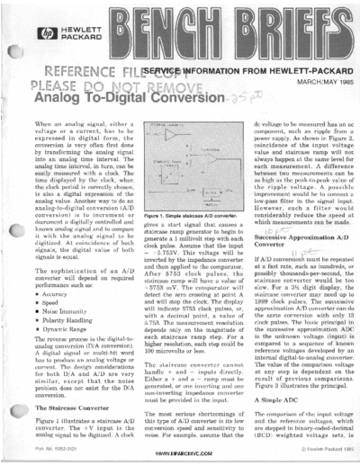
conversion) is to increment or Figure 1. Simple staircase A/D converter. considerably reduce the speed at
decrement a digitally controlled and gives a start signal that causes a which measurements can be made.
known analog signal and to compare staircase ramp generator to begin to \c I '
it with t h e analog signal to be generate a 1 millivolt step with each Successive Approximation A/D
digitized. At coincidence of both clock pulse. Assume that the input Converter
signals, the digital value of both = +5.753V. This voltage will be 1 , ;---
signals is equal. inverted by the impedance converter If A/D conversions must be repeated
and then applied to the comparator. at a fast rate, such as hundreds, or
T h e s o p h i s t i c a t i o n of a n A/D After 5 7 5 3 clock p u l s e s , t h e possibly thousands-per-second, the
converter will depend on required staircase ramp will have a value of staircase converter would be too
performance such as: +5753 mV. The comparator will slow. For a 3% digit display, the
8 Accuracy detect the zero crossing at point A staircase converter may need up to
8 Speed and will stop the clock. The display 1999 clock pulses. The successive
Noise Immunity will indicate 5753 clock pulses, or, approximation A/D converter can do
with a decimal point, a value of the same conversion with only 13
Polarity Handling 5.753. The measurement resolution clock pulses. The basic principal in
8 Dynamic Range depends only on the magnitude of the successive approximation ADC
The reverse process is the digital-to- each staircase ramp step. For a is the unknown voltage (input) is
analog conversion (D/A conversion). higher resolution, each step could be compared to a sequence of known
A digital signal or multi-bit word 100 microvolts or less. reference voltages developed by an
has to produce an analog voltage or internal digital-to-analog converter.
current. The design considerations The staircase converter cannot The value of the comparison voltage
for both D/A and A/D a r e very handle + and - inputs directly. at any step is dependent on the
s i m i l a r , except t h a t t h e noise Either a + and a - ramp must be result of previous comparisons.
problem does not exist for the D/A generated, or one inverting and one Figure 3 illustrates the principal.
conversion. non-inverting impedance converter
must be provided in the input. A Simple ADC
The Staircase Converter
The most serious shortcomings of The comparison of the input voltage
Figure 1 illustrates a staircase A/D this type of A/D converter is its low and the reference voltages, which
converter. The + V input is the conversion speed and sensitivity to are stepped in binary-coded-decimal
analog signal to be digitized. A clock noise. For example, assume that the (BCD) weighted voltage sets, is
Pub. NO.5952-0121 @ Hewlett-Packard 1985
WWW.HPARCHIVE.COM
-
V INPUT The remaining approximation is
easy to follow. Steps 100, 40, and
20 will remain switched on
(100 + 40 + 20 = lSO), then step '?
4, and finally step 1 mV
(100+40+20+4+1=165). All other
steps will be rejected. The display
logic now checks which BCD steps
have been retained and digitally
N N+l N+2
expresses the value of the analog
SUCCESSIVE NEA~UREHENTS
input.
Figure 2. Effect of noise on successive measurements.
T h e difference between t h e
converted 165 mV and the known
input of 165.5 mV is known as
quantizing error. This error results
because there is no combination of
step voltages in this particular ADC
that will yield the precise value,
that is, the ADC cannot "resolve"
the value of 0.5 mV. While another
ADC with greater resolution could
be used, it may not be as fast.
Effect of Noise
If there is noise on the input to the
Figure 3. Successive approximation A/D converter (positive voltages only). ADC, it will destroy the integrity of
the reading. Any ripple voltage '")
made at point A, which is also the of 100 mV and 80 mV is more than superimposed on the input will also
input of a comparator. Each voltage the input voltage, so the 80 mV step produce a reading error. This tells
s e t is generated i n a n 8,4,2,1 is rejected. Then the next step, now us t h a t we must hold the input
sequence and collectively represents 40 mV, is added to the 100 mV voltage constant before making the
a significant digit of the display. previously k e p t a n d t h e new analog-to-digital conversion: there
The output of the comparator drives comparison is made at 140 mV. must be a good sample and hold
the switches t h a t t u r n the BCD circuit in front of the ADC.
voltage steps on or off. If t h e The input voltage (165.5 mV) is
switched-in BCD level is more than more than the 140 mV so the 40 mV ADC With Sign Information
the input, it is rejected and the next is also kept and now the reference is
step is checked. 140 mV. This process continues The previous example assumed a
through steps 20 mV, 10 mV, 8 mV, positive input voltage. In order to
For example (refer to Figure 3), if etc. convert a negative voltage into a
the input voltage is 165.5 mV, the
ADC first compares the input value CONP
with the 1000 mV step. Since the +PO00 OFF5ET
input value is lower, the 1000 mV CONTKT BRIYE ( KEEP - RE~ECT)
A
s t e p is rejected. T h e i n p u t is +V INPUT A h r
l r
compared w i t h t h e n e x t s t e p
voltage, in this case 800 mV. The
800 mV step is also rejected for the
same reason. This comparison and
rejection is continued until the 100
mV step is compared. This com-
parison shows t h a t the input is
higher so the 100 mV step is saved.
The next step voltage is now added
to the 100 mV step just saved and
compared with the input. The total Figure 4. Successive approximation A/D converter with negative input capability.
2 BENCH BRIEFS MARCH-MAY 1985
WWW.HPARCHIVE.COM
digital code, a slight modification is
made to the circuit. Figure 4 shows
the modification.
First, an additional 2000 count step
is added. Second t h e n e g a t i v e
comparator input, instead of being
connected to ground, is connected to
a voltage t h a t simulates a 2000
count offset. This 2000 count offset
(% full scale) causes a code of 2000
to correspond to analog zero and a
code of all zeros to correspond to
- FULL SCALE ANALOG ZERO + FULL SCALE
negative full scale (see Figure 5). -DISPLAY _ .
. __t -
3435-8 4512
This example is taken from the HP
3437A System Voltmeter. T h e Figure 5. BCD code offset.
3437A is a 3-% digit (4000 count)
instrument, the highest display
being 5 1998 or approximately 4000
counts.
INPUT VOLTAGE '1 "REJECT"
The following description is loosely 1
"K E EP"
based on the HP 3437A System
Voltmeter theory of operation. Much
has been condensed, combined and I \
reworded for brevity and simplicity. I COMPARATOR
I DECISIONS
W
A Zero Input Voltage c
a
r
W
I I
I
I I I
Assume t h a t each count is t h e
equivalent t o 1 mV. The com- I 1
I
2
I
I
3
I
1
4
I
parator h a s a +2000 mV offset c
(2000 counts) hardwired to i t s CLOCK PERIOD
negative input. Therefore, with a O V I I I I I
input at point A, the comparator I I I I I
output is positive and will switch on CLOCK
t h e highest BCD bit, which i s ( I u u_
u Iu i I
-2000. The -2000 and the +2000 START CONVERT
II I
IKEEP
I I I I
at the inputs of the comparator will I
1 I I I
offset its input to zero. This will tell COMPARATOR OUTPUT I I I I I REJECT I
the switching logic t o keep the I I
I I I
-2000 bit switched on. Switching on I II II I I
the next significant bit will make Q1 I I I
I
t h e o u t p u t of t h e c o m p a r a t o r I I I I I
I
negative, which will trigger a reject
of t h i s bit. This procedure will
Q2 I I
I
JI
I I I
continue down to BCD step 1. All Q3 I I I I
bits will be rejected except t h e I I I I I
-2000 BCD bit at the beginning. BCO CODE I I Q I
O 01 I Q2 I Q3
Since the instrument contains an
algorithm that subtracts 2000 from
the value of the retained BCD steps BCD CODE
aRer the conversion, the sum is zero
and so is the display.
f A Positive Input Voltage 1 0 0 1
As an example, the input voltage at
point A shall be +500 mV, which, Figure 6. BCD code generation.
MARCH-MAY 1985 BENCH BRIEFS 3
WWW.HPARCHIVE.COM
when added to the +2000 mV offset, t h e conversion process t h a t When the algorithm subtracts 2000
totals +2500 mV. The switching generates the first four bits of the from the reading, its logic tells it
logic must keep the -2000 step BCD code for a positive input. that because the -2000 mV step
(sign), reject the -1000 and -800 was not used, the input voltage is rl
steps, and keep the -400 and -100 A Negative Input Voltage negative and that the BCD reading
mV steps to make the comparator (500) must be subtracted from 2000.
output zero (+2500 mV). However, If the input at point A is -1500 mV, The input voltage is, therefore,
when the algorithm subtracts 2000 the comparator sees an imbalance of 2000-500 = 1500. The logic adds the
from the reading, its logic tells it +500 mV (+2000 and -1500 mV). negative sign because the BCD 2000
that since the -2000 step needed to The switching logic first switches in s t e p w a s not needed t o r e a c h
be used, the input voltage is zero or the -2000 mV step, but because the balance, so the reading is -1500. In
positive. After subtracting 2000 comparator's output goes negative, all cases, that of zero input, plus
from the original 2500, the retained it is rejected. Then the -400 and input, or negative input, the digital
BCD steps are the 400 and 100, -100 mV BCD steps are switched in reading is indicated by recording
which equals 500. Figure 6 shows and all other steps are rejected. which BCD steps have been kept. U
A Refresh I;-
I
Jim Bechtold, Editor
Removing integrated circuits from a
printed circuit board is a necessary
p a r t of t h e technician's job. If t
improperly performed, the result
can be a ruined board. Therefore, it
is important that whatever method
you choose, you do it with care and
precision. We hope that reviewing
the following methods will provide
you with an interesting solution to
your IC removal job.
Figure 1. "Clip Out Method." Each lead is Figure 2. The leftover pins are removed
cut off as close to the body of the with soldering iron and needle-nose pliers.
Clip Out component as possible. A little new solder applied to the
connection will improve the heat transfer
board. Many people prefer t h i s and make the pin easier to remove.
Over the past years, Bench Briefs
method for multilayer or other
h a s explored s e v e r a l ways of
delicate boards.
removing ICs. One of the first we
showed was t h e "clip o u t " Vacuum Device
method-where each pin is cut as
close as possible to the body of the Another method removes the IC
IC (see Figure 1). The IC is then intact. Unsolder each lead of the IC
removed, leaving all the pins still by heating it on one side and using
soldered in the board. The pins can the soldersucker on the other side
be removed one at a time by heating (see Figure 3). When the IC lead
them with a soldering iron and goes through a plated-through-hole,
Figure 3. Excess solder is removed from
pulling them out with long nose it must be completely dislodged. the holes with a hand-operated vacuum
pliers (see Figure 2). Excess solder is T h i s i s accomplished, a f t e r device. A little new solder applied to the
cleared from the holes with a n unsoldering by wiggling each lead connection will cause a quicker flow and
make the solder easier to remove.
antistatic soldersucker. gently with long nose pliers. A
distinctive click will be heard as the apply the soldersucker. Now try
Some service personnel regard the
clip out method as crude, but it is
lead breaks free. Any lead t h a t
cannot be wiggled is still soldered to
again t o wiggle the lead with the
long nose pliers. Care must be used 1
very effective, easy t o learn and the plated-through-hole and must not to overheat the board. Too much
t h e r e is m i n i m a l chance of again be unsoldered. Reheat that heat in one spot on the PC board
overheating and damaging the PC lead and add new solder, then again will cause spots, referred t o as
4 BENCH BRIEFS MARCH-MAY 1985
WWW.HPARCHIVE.COM
"measling." After all the leads are
free, the IC should easily lift off the
board.
Care must be exercised in selecting
the right soldersucker. A plastic-
barreled unit can produce static
potentials in excess of 5 kV-more
than enough to damage most IC
devices. It is also possible for the
soldersucker to release lead dust
that poses a health hazard to the
operator. The source of the exposure
can be an unfiltered vent port (the
hole located in the upper portion of
the barrel), or a defective O-ring seal
between the piston and cylinder. If
the O-ring deteriorates, solder dross
(containing lead) can migrate above
the piston to where it contaminates
the upper portion of the cylinder. Figure 5. Continuous vacuum desoldering principle.
When the piston is activated inside
a contaminated cylinder, a small
amount of lead may be blown out technician's bench-especially at a
the vent hole along with air from board repair station. One of the self-
t h e piston. D a i l y c l e a n i n g , contained systems we are using is a
lubricating and inspection of the PACE MBT-100 MicroBenchTopTM
O-ring seal should help alleviate this desoldering station. (See Figure 4;
problem. Note that the soldering iron and
holder shown on top of the station is
not part of the PACE system.) The
Desoldering System
basic desoldering principle of this
type system is shown in Figure 5.
A more elaborate and efficient tool Figure 6. Each IC lead is unsoldered
The idea is to place the temperature quickly and efficiently with the hot tiplhigh
for r e m o v i n g I C s i s called a
controlled hollow tip over the lead vacuum tool.
desoldering s t a t i o n . T h i s is a
making contact with the solder. As
temperature controlled soldering
the solder melts, allow the tip to
iron with a hollow tip connected to a Installation and Cleaning
rest on a film of solder between the
vacuum pump. A p p r o p r i a t e
pad and tip. Move the tip with a
filtering, temperature control and After the defective IC is removed
stirring motion until the lead is free
ease of handling and cleaning make and the holes are cleaned, install
and the solder is completely melted.
this an attractive addition to the the new IC. Before you solder it into
Then, keeping the tip in motion,
apply the vacuum and suck the place, double check the orientation.
melted solder from the plated-thru- It is most embarrassing to complete
hole. One word of caution though, the soldering operation only to
don't press down on the pad or you'll realize t h a t the IC is installed
suck it off the board. Continue the backwards. As you solder the new
stirring action and vacuum flow for IC in place, be certain to get each
a moment to cool the joint area. pin hot enough so solder flows up
into the plated-through-hole. Some
After all the leads are unsoldered, technicians suggest soldering the
check each one with your long nose lead from both sides of the board.
Figure 4. PACE MBT-100 MicroBenchTopTM
desoldering station. Note that the soldering pliers. Any lead that cannot be
iron and holder shown on top of the station wiggled is still soldered and must A s f a r a s cleaning, we don't
are not part of the PACE system.
again be unsoldered. As before, recommend it. Solder flux from
resolder t h e lead and t h e n go RMA-P2 solder does no harm if left
through t h e extraction process in place on a PC board after a hand
TMPACE, Inc. 9893 Brewers Ct. Laurel, MD a g a i n . Allow t h e joint t o cool soldering operation; the rosin is
20707 between resoldering and extraction. inert and nonconductive. However,
MARCH-MAY 1985 BENCH BRIEFS 5
WWW.HPARCHIVE.COM
when you dissolve i t w i t h a away. The activators a r e water
chemical, attempting to remove it soluble. If the instrument is stored
from the board, it is like pouring oil
on water; the rosin flux dissolves
and spreads all over the board,
in a humid environment, all it takes
is a little time and moisture to start
the corrosion process. For more
r
releasing its activators (chlorides, information on PC board rework,
bromides, etc.). Now instead of repair and cleaning, write to the
having a harmless blob of rosin flux editor and ask for Bench Briefs
with the activators trapped, you issue 5952-0111. 0
Figure 7. In case the isolated hot solder
have a potential time bomb ticking
path clogs, use the enclosed round wire
brush for cleaning.
Library- 5951-6511 HP 3488A SWlTCHlCONTROL UNIT
.uoy\lement t
o Subscription 5951-6517 3488A-2. Serials 2240A01857 and below. Improved
case for the HP 3488A.
Contact your local HP Sales Office HP 3561A DYNAMIC SIGNAL ANALYZER
3561A-4. 03561-66570 pulse width control assembly.
for ordering information. How to properly identify current sensing inductor
A70T600.
GENERAL 3561A-5. 2338A01370 and below. Modification to re-
5083-12. End of support for cathode ray tubes used in vision C A50 assembly to make built-in diagnostic
1331NC and 1208NB instruments, all options. test routines 150, 151, and 152 operable.
5083-14. End of support for cathode ray tubes used in 3561A-6. All serials with option 001 bubble memory.
17108. 1712A, 1720A & 1720AF instruments, all New bubble module package.
options cathode ray tube part numbers 5083-4052 3561A-7. All serials with option 001 bubble memory
& 5083-4070. modification to prevent error return code - 1 5 29989
Meed Any Service HP 181N181AR OSCILLOSCOPES
00368342.
181AiAR-12. 181A serial prefix 1324A and below; HP 3711A IF/BB TRANSMITTER
Motes? 181AR serial prefix 1337A and below. Recom-
mended replacement for the A6 pulse board
3711A-o, note index.
assembly. HP 3712A IF/BB RECEIVER
They're free! 3712A-0. Service note index.
HP 436A POWER METER
436A-9. All serials. HP-I8 verification program for HP HP 3715 BB TRANSMITTER
Here's the latest listing of service 9836 controller. 3715A-0. Service note index.
notes. They recommend modifica- HP 438A POWER METER HP 37308 DOWN CONVERTER
tions to Hewlett-Packard instru- 438A-2. All serials. Rear panel input (option 002) retrofit
37308-o, note index,
instructions.
ments t o increase r e l i a b i l i t y , HP 37378 RF MODULE
improve performance, or extend HP 1347A HP-IB DISPLAY 37378-0. Service note index.
their usefulness. 1347A-3. All serials. Instructions on segmenting the
memory in the 1347A. HP 37388 RF MODULE
373850. Service note index.
Use the order form at the rear of HP 1630A/D/G, 1631A/D LOGIC
ANALYZERS HP 37398 RF MODULE
Bench Briefs to order, free of charge, 1630ND/G-1/1631A/D-l. Serial prefix: 1630ND, 1631N 373950. Service note index.
individual service notes document- D below 2512A; 1630G below 2513A. Change to
the power-up master reset circuit to improve HP 3743A IF AMPLIFIER
ing several instruments. performance. 3743A-0. Service note index.
HP 3065 BOARD TEST SYSTEM
If you would like to purchase large 306523. All serials. Check for possible miswired DSDC HP 3746A SELECTIVE LEVEL
quantities of service notes covering internal cable. MEASURING SET
3065-24. All serials. ASRU 2410 firmware bug 3746A-0. Service note index.
a wide range of instruments, or if workaround. 3746A-14. All serials. Preferred replacement for A41E l
you desire a complete history of all 306525. Serials 2310A00364 and below. Power module crystal oscillator.
to monitor card cable miswiring 3746A-15. Serials 241OU-00602 and below. Inspection
service notes documenting a l l for short circuit between motherboard casting.
changes to your instruments, Hew- HP 3336AIBIC SYNTHESIZER/LEVEL
GENERATOR
lett-Packard offers a microfiche li- 3336NBiC-10. All serials. Relay cleaning procedure.
HP 3757A 8.5 MHz ACCESS SWITCH
3757A-0. Service note index.
brary for a modest, one time charge. 3336NBiC14.3336A serials 1930A00987 and below;
33368 serials 1931A01735 and below; 3336C serials
There is also a microfiche subscrip- 1932A00667 and below. Transistor mounting mod- HP 3762A DATA GENERATOR
tion service available that automat- ification to prevent intermittent resets and erroneous 3762A-0. Service note index.
front panel displays.
ically updates the library on a 3336NBiC-15.3336A serials 1930A01115 and below: HP 3763A ERROR DETECTOR
quarterly schedule. 33368 serials 1931A02240 and below: 3336C serials 3763A-11. Options 201, 202, 330. Preferred replace-
1932A00850and below. Recommended replacement
30 MHz reference crystal.
ment for A3Q5 and A3Q6. f-
The part numbers for the service HP 3764A DIGITAL TRANSMISSION
HP 3467A LOGGING MULTIMETER ANALYZER
note microfiche library and sub- 3467A-6. Serials 1821A01214 and below. Improved 3764A-10. All serials. Printer retrofit kit.
scription service are: common mode rejection of input amplifier. 3764A-11. All serials. Tape cassette retrofit kit.
6 BENCH BRIEFS MARCH-MAY 1985
WWW.HPARCHIVE.COM
HP 3776AIB PCM TERMINAL TEST SET HP 4945A TlMS HP 8116A PULSEIFUNCTIONGENERATOR
OPTION 001 4945A-1. Serials 2435A and below. Modification to 50 MHz
3776A-1EA. Serials 24441100292 and below. Frequency prevent power supply regulators from shorting to 8116A-1A. Serial 21246: serials 2334A00224 and be-
update instructions for data measurement option chassis. low. Modification of the output amplifier.
001. 4945A-2. Power supply modification to improve 81 16A-2. All serial numbers. New dual transistor part-
3776A-20A. Serials 24441100292 and below. Modifi- performance, number.
cation to make old assembly 03776-60008 compat- 4945A-3. Serials 2435 and below. Software upgrade
ible with firmware rev 2501. rev 2.0. HP 8165A PROGRAMMABLE SIGNAL
3776A-21. All serials. 37/6 test programs data cartridge 4945A-4. Service kit modification. SOURCE
( H P part number 03776-1 0001) modifica- 8165A-11. All serials. New dual transistor part-number.
tions - update to rev C. HP 4951A PROTOCOL ANALYZER
3776518A. Serials 24371100642 and below. Frequency 4951A-7. Serials 2443A02576 and below. SCC retrofit HP 8405A VECTOR VOLTMETER
update instructions for data measurement option kit. 8405A-10A. Serials 732A and above. Precautions to
001. 4951A-9. All serials. Final test procedure. prevent damage when handling 8405A probes.
3776B-21. All serials. 3776 test programs data cartridge 4951A-10. Serials 2443A and below. Software revision
( H P part number 03776-10001) modifica- 2.0. HP 8620C SWEEP OSCILLATOR
tions - update to rev C.
86200-9. Serials 2252a and below. Fan assembly and
HP 4953A PROTOCOL ANALYZER operation control assembly replacement kit.
HP 3779AIB PRIMARY MULTIPLEX 4953A-1. Serials 2441A00326 and below (see table in
ANALYZER contents of note). Modification to fix handle mounting HP 8662A SYNTHESIZED SIGNAL
rails. GENERATOR
3779A-36. All serials. Preferred replacement for tran-
4953A-2. Serials 2441A and below prefix (see table in 8662A-12. Serials 2424A and below. Modification to
sistors Q4 and Q8 on the A29 assembly.
contents of note). Power supply modification to im- improve low frequency loop performance and elim-
37798-38. All serials. Preferred replacement for tran-
prove performance. inate intermittent status errors 03/04.
sistors Q4 and Q8 on the A29 assembly.
4953A-3. Serials 2441A and below (see table in contents 8662A-13. Serials 2509A and below. Modification to
37798-39. All serials. Preferred ROM U31 and 1141
of note). 2.1 firmware update. prevent fuse blowing during power up in 23OVAC
replacement on the A24 assembly.
4953A-4. Serials 2441A00291 and below (see table in mode.
contents of note). A6 and A19 memory board U707
HP 3779CID PRIMARY MULTIPLEX IC change. HP 8663A SYNTHESIZED SIGNAL
ANALYZER GENERATOR
37790-21. Serials 309 to 403. Improved return loss HP 5328AI5328AH99 UNIVERSAL 8663A-7. Serials 2507A and below. Modification to
measurement performance, COUNTER prevent fuse blowing during power up in 23OVAC
3779C-22. Serials 458 and below. Preferred replace- 5328A-41. All serials for the 5328A; serials 2424 and mode.
ment for assemblies A23, A24, A25 and A26. below for the 5328AH99. Modification to turn off the
3779D-25. Serials 244 to 333. Improved return loss fan in standby mode. HP 8673BlCID SYNTHESIZED SIGNAL
measurement performance. GENERATOR
3779D-26. Serials 438 and below. Preferred replace- HP 53286 UNIVERSAL COUNTER 86736-2. Serials 2447A and below. Firmware update
ment for assemblies A23, A24. A25 and A26. 53288-2. Serials 2424 and below. Modification to turn kit.
off the fan in standby mode. 8673C-2. Serials 2452A and below. Firmware update
HP 3780A PATTERN GENERATORIERROR kit.
DETECTOR HP 5342A MICROWAVE FREQUENCY 8673D-2. Serials 2449A and below. Firmware update
3780A-30. Options 100 and 101. Preferred replacement COUNTER kit.
for A1305 and A13Q6. 5342A-42. Serials 2440A09236 and below. Modification
to prevent high frequency miscount. HP 86846 SIGNAL GENERATOR
5342A-43. Serials 2428A8916 to 2440A9306. Rec- 86846-2. All serials. Power amplifier oscillation troub-
HP 3782A ERROR DETECTOR ommended IC replacement to prevent miscounts. leshooting hint.
3782A-5. All serials. Preferred replacement for A32Q12
and A32Q13. HP 1W04D, 10005D, 1W06D, 10013A,
HP 5343A MICROWAVE FREQUENCY 10014A AND 100168 1O:l VOLTAGE
COUNTER DIVIDER PROBES AND HP 10007B AND
HP 3785AIB JITTER GENERATOR &
5343A-21. Serials 2428A1736 to 2440A1956. Rec- 10008B VOLTAGE PROBES (PASSIVE)
RECEIVER
ommended IC replacement to prevent miscounts. 100XXAIBID-1. Possible probe accessory tips shorting
3785A-14. All serials. Retrofit instructions for option
062. to ground internally.
HP 5345A ELECTRONIC COUNTER
3785A-16. All serials. Preferred replacement for
5345A-26. Serials 2242Al0310 and below. Instructions
A 11U33. HP 117298 CARRIER NOISE TEST SET
to retrofit a standard HP 5345A to option 012 (original
37856-13. All serials. Retrofit instructions for option
version front end). 1 17296-3. Serials 2345A and below. Modification to
062.
5345A-27. Serials 2242A10311 and above. Instructions improve A7C5iC8 reliability.
to retrofit a standard HP 5345A to option 012 (new
HP 4062A SEMICONDUCTOR version front end). HP 64100A LOGIC DEVELOPMENT
PARAMETRIC TEST SYSTEM STATION
4062A-5 All serials Instal alion informat,on for the HP 6011A SYSTEM POWER SUPPLY 64100A-14. Serials 2210A thru 2336A, all 64100 to
16294A field Lpgrade &it 601 1A-1. Serials 2530A00211 and above. Modification 66524 and 69524 rear panel boards. Modification
to increase reverse voltage protection. to prevent intermittent system bus failures.
HP 4274A MULTI-FREQUENCY LCR HP 6012A SYSTEM POWER SUPPLY HP 64610s HIGH SPEED TIMINGISTATE
METER 6012A-6. Serials 2426A02636 thru 2426A2891 and ANALYZER
4274A-26. Serials 2434J02741 and below. Bias circuit 2426A02910. Recommended meter replacement. 646016-1. All serials. 125 MHz time state module cal-
modification for new replacement FET. ibration procedure.
HP 6031A SYSTEM POWER SUPPLY
6031A-2. Serials 2508A00243 and above. Modification HP 69791A AND 69792A HIGH SPEED
HP 4937A TRANSMISSION IMPAIRMENT to increase reverse voltage protection. MEMORY CARDS
TEST SET 69791A-1169792A-1. All serials. Documentation cor-
4937A-1. Serials 2418 and below. Modification to im- HP 6942A AND 6944A rections for memory card verification routines.
prove the hold circuit. MULTIPROGRAMMERS
6942A-1016944A-1. All serials. Field support kit HP 86601A RF SECTION PLUG-IN
description. 86601A-9. Serials 2437A and below. Modification to
HP 4938A NETWORK CIRCUIT ACCESS improve reliability of A13 attenuator assembly.
TEST SET HP 7090A MEASUREMENT PLOlllNG
4938A-1. Serials 2450A and below. Corrected REN-3 SYSTEM HP 866026 RF SECTION PLUG-IN
load. 7090A-2. Serials 2418A & 2430A. Design changes to 866028-4. Serials 2437A and below. Modification to
7090A power supply PCA. improve reliability of A13 attenuator assembly.
HP 4944A TlMS HP 8111A PULSEIFUNCTIONGENERATOR HP 86603A RF SECTION PLUG-IN
4944A-12A. Serials 2027A00899 and below. Self check 20MHz 86603A-6. Serials 2446A and below. Modification to
failures under coolidamp conditions. 81 11A-2. All serials. New dual transistor part-number. improve reliability of A13 attenuator assembly.
MARCH-MAY 1985 BENCH BRIEFS 7
WWW.HPARCHIVE.COM
rice Note Order
! For European customers (ONLY) Name r
1 Hewlett-Packard Firm
Central Mailing Dept.
P. 0. Box 529
Van Hueven Goedhartlaan 121 City
AMSTELVEEN-1134
State Zip
Netherlands
0 37798-39 0 4951A-9 0 8111A-2 .
0 3779C-21 0 4951A-10 0 8116A-1A
0 3779022 0 4953A-1 0 8116A-2
0 3779025 0 4953A-2 0 8165A-11
4
0 3779D-26 0 4953A-3
8405A;\10A
0 3780A-30 0 4953A-4 0 86200s\,
0 3782A-5 0 5083-12 0 8662A-12,
0 3785A-14 0 5083-14 0 866249-13 4
0 3785A-16 0 5328A-41 0 8663A-7 \
0 37858-13 0 53288-2 0 86738-2
\
0 4062A-5 0 5342A-42 0 867302
0 4274A-26 0 5342A-43 0 867302 \
0 4937A-1 0 5343A-21 0 86848-2
0 4938A-1 0 5345A-26 0 lOOXXAIB/D-l
0 4944A-12A 0 5345A-27 0 117298-3
0
0
0
4945A-1
4945A-2
4945A-3
0
0
0
6OllA-1
6012A-6
6031A-2
0 641OOA-14
0 646018-1
0 69791A-1169792A-1
r.
0 4945A-4 0 6942A-1016944A-1 0 86601A-9
0 4951A-7 0 7090A-2 0 866028-4
0 86603A-6
Please photocopy this order form if you do not
want to cut off the page
Bulk Rate
U.S Postage
Sunnyvale. CA.
Permit No.
All rights reserved Permission lo reprint Bench Briefs granted upon written request to the Editor Printed in U S A .
WWW.HPARCHIVE.COM
◦ Jabse Service Manual Search 2024 ◦ Jabse Pravopis ◦ onTap.bg ◦ Other service manual resources online : Fixya ◦ eServiceinfo