Service Manuals, User Guides, Schematic Diagrams or docs for : Intel Legacy Package_databook_1999 ch_11
<< Back | HomeMost service manuals and schematics are PDF files, so You will need Adobre Acrobat Reader to view : Acrobat Download Some of the files are DjVu format. Readers and resources available here : DjVu Resources
For the compressed files, most common are zip and rar. Please, extract files with Your favorite compression software ( WinZip, WinRAR ... ) before viewing. If a document has multiple parts, You should download all, before extracting.
Good luck. Repair on Your own risk. Make sure You know what You are doing.
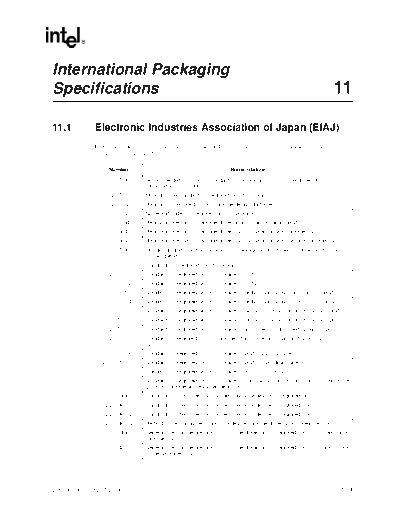
Image preview - the first page of the document

>> Download ch_11 documenatation <<
Text preview - extract from the document
International Packaging
Specifications                                                                                                       11

11.1          Electronic Industries Association of Japan (EIAJ)
              EIAJ publishes the following rules and standards as they apply to the preparation of outline
              drawings of integrated circuits.

                   Number                                              Nomenclature

                  ED -7300       Recommended practice on standard for the preparation of outline drawings of
                                 semiconductor packages
                  ED -7301       Manual or the standard of integrated circuits package
                  ED -7302       Manual for integrated circuits package design guideline
                  ED -7303       Name and code for integrated circuits package
                  ED -7304       Measuring method for package dimensions of ball grid array (BGA)
                  ED -7304-1     Measuring method for package dimensions of Small Outline Package (SOP)
                  ED -7304-2     Measuring method for package dimensions of Small Outline J-leaded package (SOJ)
                  ED -7305       Unit design guide for the preparation of package outline drawing of integrated circuits
                                 (gullwing-lead)
                   ED -7311      Standards of integrated circuits package
                  ED -7311-1     Standard of integrated circuits package [TSOP(1)]
                  ED -7311-2     Standard of integrated circuits package [TSOP(2)]
                  ED -7311-3     Standard of integrated circuits package [Tape Ball Grid Array 1.0mm pitch (T-BGA)]
                  ED -7311-4     Standard of integrated circuits package [Tape Ball Grid Array 1.27mm pitch (T-BGA)]
                  ED -7311-5     Standard of integrated circuits package [32/48 pins Fine-pitch Ball Grid Array (FBGA)]
                  ED -7311-6     Standard of integrated circuits package [60/90 pins Fine-pitch Ball Grid Array (FBGA)]
                  ED -7311-7     Standard of integrated circuits package [Plastic Fine pitch Ball Grid Array (P-FBGA)]
                  ED -7311-8     Standard of integrated circuits package [Plastic Fine pitch Ball Grid Array 0.8mm pitch (P-
                                 FBGA)]
                 ED -7311-9A     Standard of integrated circuits package [P-BGA (Cavity up type)]
                ED -7311-10A     Standard of integrated circuits package [P-BGA (Cavity down type)]
                 ED -7311-11A    Standard of integrated circuits package (119/153 pins P-BGA)
                 ED -7311-12     Standard of integrated circuits package (52 pins 64 pins 80 pins and 100 pins low-profile
                                 quad flat package with exposed heatsink)
                  ED -7400       Standards for the dimensions of semiconductor devices (integrated circuits)
                  ED -7400-1     Standards for the dimensions of semiconductor devices (integrated circuits)
                  ED -7400-2     Standards for the dimensions of semiconductor devices (integrated circuits)
                  ED -7401-4     Method of measuring semiconductor device package dimensions (integrated circuits)
                  ED -7405       General rules for the preparation of outline drawings of integrated circuits zigzag in-line
                                 packages (ZIP)
                  ED -7405-1     General rules for the preparation of outline drawings of integrated circuits shrink zigzag
                                 in-line packages (SZIP)


2000 Packaging Databook                                                                                                  11-1
International Packaging Specifications


                  ED -7406A     General rules for the preparation of outline drawings of integrated circuits small outline J-
                                lead packages (SOJ)
                  ED -7408A     General rules for the preparation of outline drawings of integrated circuits pin grid array
                                packages (PGA)
                   ED -7414     General rules for the preparation of outline drawings of integrated circuits guarding quad
                                flat packages (GQFP)
                   ED -7415     General rules for the preparation of outline drawings of integrated circuits small outline
                                packages with heat sink (HSOP)
                   ED -7417     General rules for the preparation of outline drawings of integrated circuits bumpered
                                quad flat packages (BQFP)
                   ED -7418     General rules for the preparation of outline drawings of integrated circuits glass sealed
                                quad flat packages (QFP-G)
                   ED -7419     General rules for the preparation of outline drawings of integrated circuits glass sealed
                                dual in-line packages (DIP-G)
                   ED -7421     General rules for the preparation of outline drawings pf integrated circuits ceramic dual
                                in-line packages (DIP-C)
                   ED -7422     General rules for the preparation of outline drawings of integrated circuits glass sealed
                                quad flat J-leaded packages (QFJ-G)
                   ED -7423     General rules for the preparation of outline drawings of integrated circuits ceramic quad
                                flat J-leaded packages (QFJ-C)
                 ED -7431-1A    Recommended outline drawings for carriers quad tape carrier packages (QTP carrier)
                  ED -7431A     General rules for the preparation of outline drawings of integrated circuits quad tape
                                carrier packages (QTP)
                   ED -7432     General rules for the preparation of outline drawings of integrated circuits dual tape
                                carrier packages (type1) (DTP(1))
                   ED -7433     General rules for the preparation of outline drawings of integrated circuits dual tape
                                carrier packages (type 2)
                  ED -7441B     Standard for the package of universal memory devices
                  ED -7500A     Standards for the dimensions of semiconductor devices (discrete semiconductor devices)
                  EDR-7311      Design guideline of integrated circuits for quad Flat package (QFP)
                  EDR-7312      Design guideline of integrated circuits for thin small outline package (type1)
                  EDR-7313      Design guideline of integrated circuits for thin small outline package (type 2) (TSOP2)
                  EDR-7314      Design guideline of integrated circuits for shrink small outline package (SSOP)
                  EDR-7315A     Design guideline of integrated circuits for ball grid array (BGA)
                  EDR-7316      Design guideline of integrated circuits for Fine-pitch Ball Grid Array and Fine-pitch Land
                                Grid Array (FBGA/ FLGA)
                  EDR-7317      Design guideline of integrated circuits for Surface Vertical Package (SVP)
                  EDR-7318      Design guideline of integrated circuits for plastic very thin small outline non-lead package
                                (P-VSON)
                  EDR-7319      Design guideline of integrated circuits for quad flat J-lead packages (QFJ)
                  EDR-7320      Design guideline of integrated circuits for small outline package (SOP)
                  EDR-7601      Guidance of embossed carrier taping for integrated circuits


11.2          Joint Electron Device Engineering Council (JEDEC)
              JEDEC Publication 95 lists all package outlines. More information about JEDEC can be located on
              their web site at http://www.jedec.org.


11-2                                                                                          2000 Packaging Databook
                                                                      International Packaging Specifications


11.3          Mil Standards
              The following military standards include specifications required to meet U. S. Military
              requirements.
◦ Jabse Service Manual Search 2024 ◦ Jabse Pravopis ◦ onTap.bg ◦ Other service manual resources online : Fixya ◦ eServiceinfo