Service Manuals, User Guides, Schematic Diagrams or docs for : Keithley 500 500_932_01C
<< Back | HomeMost service manuals and schematics are PDF files, so You will need Adobre Acrobat Reader to view : Acrobat Download Some of the files are DjVu format. Readers and resources available here : DjVu Resources
For the compressed files, most common are zip and rar. Please, extract files with Your favorite compression software ( WinZip, WinRAR ... ) before viewing. If a document has multiple parts, You should download all, before extracting.
Good luck. Repair on Your own risk. Make sure You know what You are doing.
Image preview - the first page of the document
>> Download 500_932_01C documenatation <<
Text preview - extract from the document
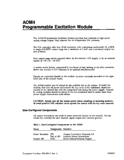
AOM4
Programmable Excitation Module

          The AOM4 Programmable Excitation Module provides four channels of high-speed
          anaIog voltage output. Each channel has an independent D/A converter.


          The D/A converters offer true X&bit resolution with a maximum nonlinearity of *.0X!%.
          A single 0-10.2375Voutput range has a resolution of 2.5mV and a maximum output cur-
          rent of 4OmA.


          Each output stage can be supplied either by the internal +l5V supply, or by an external
          supply of +l5 (+2, -0) VDC.


          A system strobe feature, supported by two levels of data latching in the D/A converters,
          allows any number of D/A channels to be updated simultaneously.


          Signals are connected directly to the module via screw terminals mounted on the right-
          hand side of the module board.


          The AOM4 module may be placed in any available slot in the system. To install the
          module, first turn off power and remove the top cover of the mainframe. Insert the
          module in the desired slot with the component side facing the power supply. General-
          ly, analog modules should be placed in the low-numbered slots to isolate them from
          power supply thermal and noise effects.


          CAUTION: Always turn off the system power before installing or removing modules.
          To avoid possible EM1 radiation never operate the system with the top cover removed.


User-Configured    Components

          All output connections are made to screw terminals located on the module. Two ter-
          minals are provided for each channel: signal output and common ground.


          Table 1. User-Configured Components on the AOM4

          Name              Designation     Function

          Screw Terminals   Jl7'l           Output Connection Channels O-3
                            Part of Jl.7l   External Power Connections
          Jumper 101        WlOl            Select Internal/External Supply


Document Number: 500-932-01 Rev. C                                                        AOM4-1
        Figure 1. AOM4 Module


AOM42
       Connections

       Terminal connections are shown in Figure 2, which illustrates a typical connecting
       scheme. The use of shielded cable is recommended to minimize the possibility of EM1
       radiation. Connect one end of the shield to AOM4 ground and leave the other end
       disconnected.


                                         J---J-+      EXTERNAL SUPPLY,


                           IL!8      I","I      (SEE TEXT FOR MAXIMUM    VALUE)


       Figure 2. Typical AOM4 Output Connections           (Channel 0 shown)


       Voltage Supply Connections

       The channel outputs may be operated from either the internal +l5V supply or an exter-
       nal supply of +l5 (+2, -0) VDC. When using the internal supply, jumper WlOl must
       be in the INT position. To operate the module on an external supply, place WlOl in the
       EXT position and connect the supply to the external supply terminals. Be sure to
       observe proper polarity.


       Output Loading Considerations

       Each channel on the AOM4 card can supply a maximum of lO.2375V at 40mA. Thus
       there is a minimum resistance value that can be conconnected across the outputs
       without loading them down. With the above voltage and current values, the minimum
       recommended load resistance is 25612.Note that the outputs are short circuit protected,
       so that lower resistance values will not damage the module, but they will affect output
       accuracy. However, the maximum recommended load capacitance is O.&S. Exceeding
       this value may cause the output channel to oscillate.


Commands

       AOM4 module commands are listed in Table 2. Table 3 summarizes the locations for
       slot-dependent commands.

                                                                                       AOM4-3
         Table 2. Commands Used with the AOM4 Module

         Command                   Location

         D/A CONTROL               Slot-dependent CMDA
         D/A DAL4                  Slot-dependent CMDB
         STROBE                    CFF9D


         Table 3. Locations of Slot-dependent Commands

         Slot           CMDA         CMDB

         Slot   1       CFFSO
         Slot   2       CFF82
         Slot   3       cFF84
         Slot   4       CFF86
         Slot   5       CEE88
         Slot   6       cFF8A
         Slot   7       CFF8C
         Slot   8       CFF8E
         Slot   9       CFF90
         Slot   lo      CFF92


         D/A CONTROL

         Location: Slot-dependent CMDA

         D/A CONTROL always precedes D/A DATA, indicating to the AOM4 module which
         channe1 of analog output to update, and which byte of data to load. Table 4 lists values
         written to the D/A CONTROL locations.


         The high and low bytes of data may be updated independently and in any order; there
         is no hardware reason that both bytes must be updated at the same time. Similarly,
         channels can be updated independently and in any order.


         The location assigned to D/A CONTROL varies depending on which baseboard slot
         holds the D/A converter being addressed (See Table 3).


         Table 4. Values Written to D/A CONTROL

         Function                    Binary   Hex    Decimal

         Channel     0 low byte      0000     HO     0
         Channel     0 high byte     0001     Hl     1
         Channel     1 low byte      0010     H2     2
         Channel     1 high byte     0011     H3     3
         Channel     2 low byte      0100     H4     4
         Channel     2 high byte     0101     H5     5
         ChanneI     3 low byte      0110     iz;    7
                                                     6
         Channel     3 high byte     0111


AOM4-4
DIA Dp;TA

Location: Slot-dependent CMDB

D/A DATA is used to load data values into the D/A converter. This command should
always be preceded by D/A CONTROL, which selects the channel and the byte to be
loaded. The data must be separated into low and high bytes prior to loading, and each
byte must be prefaced by D/A CONTROL.


When the strobe feature is not enabled, the output of the converter is updated im-
mediately. Thus, when the strobe is not used, the low and high bytes are updated in-
dependently. When the strobe is enabled, outputs are not updated until the STROBE
command is issued with the value 1 (to issue data).


To determine the digital value to input for a given voltage, it is necessary to know the
output range of the D/A converter. With a l2-bit digital converteI; there are 4096 possi-
ble voltage levels, specified with digital values O-4095.Therefore the actual voltage of
each step equals the range divided by 4095. For an input range of 0 to 10.237V the
voltage of each step is 10237V/4095 or 2.5mV: thus a BASIC formula for each voltage
value can be derived:


Where V is voltage and D is the digital value in counts loaded into the converter.
Similarly, the following BASIC equation determines the digital value to use when a par-
ticular voltage is required:

                 V
D=   INT (
             2.5 x 10-j


Again, D is the digital value, while V is the voltage.


The digital values may be separated into low byte (LB) and high byte (HB) values with
the following equations:

HB = INT (D/256)
LB =(D/256-HB) l 256


STROBE

Location: CFF9D

The STROBE command is used to make possible the synchronous updating of two or
more analog output channels. STROBE is issued in three modes: strobe enable, strobe
disable and issue data. The STROBE feature must either be enabled or disabled at the
start of any program, or the D/A converters will not function (see Table 5).


When any strobe feature is disabled, all data given to a D/A converter is immediately
placed in that converter's primary data latch, and the current output updated. The low
byte and high byte are thus updated asynchronously


                                                                                  AOM4-5
        When the strobe is enabled, no data is updated until the STROBE command has been
        issued in the issue data mode. New data is placed in a secondary data latch within the
        D/A converter. When the STROBE command (to issue data) is given, new data is releas-
        ed to the primary data latch, updating the voltage output, and old data in other chan-
        nels is reissued, leaving the voltage output of these channels unchanged. The strobe is
        completely flexible. Any amount of data-from a single byte to any number of channels-
        can be updated when the strobe is enabled.


        To use the strobe, issue the strobe enable command early in the program. Use the D/A
        CONTROL and D/A DATA commands to load the secondary latches of the appropriate
        converters. This can be done as far in advance as required. To issue the new data, load
        STROBE with 1 (to issue data), releasing all data loaded since the last issue data com-
        mand and leaving unchanged the outputs of other channels.


        The STROBE feature is global, affecting all D/A modules installed in the Series 500
        simultaneously.


        Table 5. Values Written to STROBE

        Function            BillarV        HeX     Decimal

        Strobe Enable       01000000       H40     64
        Strobe Disable      10000000       H80     128
        Issue Data          00000001       HO1     1


AOM4 Module Calibration

        Calibration of the AOM4 module is very similar to the procedure used to calibrate the
        AOMl. This module has only a single range, howevel; so the complexity is reduced
        considerably. Figure 3 shows calibration adjustment locations for the AOM4 Program 1
        lists a calibration program intended for use with this module.

        1. Place the module to calibrated in slot 5 of the system baseboard.
        2. Unless an external voltage source is connected to the module, place the supply
           jumper in the internal position.
        3. Connect the DMM high (or current input)lead to the signal output terminal of the
           channel being calibrated. Connect the DMM low signal lead to module ground.
        4. Select an appropriate function and range on the DMM. Remember that the AOM4
           output signal is a voltage in the range of 0 to +10.2375V.
        5. Enter program 1 into the computer.
        6. Run the program and follow the instructions given. The program will prompt for
           module type and output channel, and then display the correct offset and gain adjust-
           ment values in that order.


AOM46
                                                CHAN   0 OFFSET
                                                CHAN   0 GAIN


                                                CHAN   1 OFfWFT
                                                CHAN   1 GAIN

                                         &g-J   CHAN   2 OFFSET
                                         ,,     CHAN   2 GAIN


                                                CHAN    3 OFFSET
                                                CHAN    3 GAIN


Figure 3. AOM4 Calibration Adjustments


                                                                   AOM47
         Program 1. AOM4 Calibration

         10 DEF SEG=&HCFFO:CLS
         20 CA=&H88:CB=&H89:ST=&H9D
         30 POKE ST,64
         40 PRINT"1-AOM3"
         50 PRINT"2-AOM4'
         60 PRINTzINPUT `MODULE TYPE (1 OR 2)";M
         70 IF M2 THEN 60
         80 IF M=l THEN M$="AOM3":R$="CURRENT"
         90 IF M=2 THEN M$=`AOM4":R$="VOLTAGE"
         100 PRINT "INSERT";M$:"INTO SLOT 5"
         110 PRINT:INI'UT "CHANNEL (0-3)";CH
         120 IF CH3 THEN 110
         130 PRINTPRINT "CONNECT DMM To CHANNEL';CH
         140 PRINT "SET DMM TO MEASURE";R$
         150 ON M GOSUB 300,320
         160 POKE CA,2*CH:POKE C&LB
         170 POKE CA,TCH+lzPOKE CB,HB
         180 POKE ST,1
         190 PRINTPRINT'ADJUST CHANNEL';CH;"OFFSET FOR"; L$;"READING ON DMM"
         200 INPUT "PRESS RETURN To CONTINUE";A$
         210 ON M GOSUB 310,330
         220 POKE CA,2*CH:POKE CB,LB
         230 POKE CA,2*CH+l:POKE CB,HB
         240 POKE ST,1
         250 PRINTPRINT'ADJUST CHANNEL";CH;"GAIN  FOR";H$; `READING ON DMM"
         260 INWT'TRESS RETURN To CONTINUE";A!$
         270 PRINTzINI'UT'AGAIN";A!$
         280 IF LEFl?
◦ Jabse Service Manual Search 2024 ◦ Jabse Pravopis ◦ onTap.bg ◦ Other service manual resources online : Fixya ◦ eServiceinfo