Service Manuals, User Guides, Schematic Diagrams or docs for : LG Mobile Phone LG G5200 LG G5200 13
<< Back | HomeMost service manuals and schematics are PDF files, so You will need Adobre Acrobat Reader to view : Acrobat Download Some of the files are DjVu format. Readers and resources available here : DjVu Resources
For the compressed files, most common are zip and rar. Please, extract files with Your favorite compression software ( WinZip, WinRAR ... ) before viewing. If a document has multiple parts, You should download all, before extracting.
Good luck. Repair on Your own risk. Make sure You know what You are doing.
Image preview - the first page of the document
>> Download LG G5200 13 documenatation <<
Text preview - extract from the document
3. TECHNICAL BRIEF
3. TECHNICAL BRIEF
3.1 General Descreption
The RF parts consists of a transmitter part,a receiver part,a synthesizer part,a voltage supply part,a
VCTCXO part. And the main RF Chipset CX74017[U411]is a single-chip dual-band transceiver for
the extended global system for mobile communication[E- GSM900MHz]/Digital communication
system[DCS1800MHz] voice and data transfer applications.
This device integrated a direct conversion receiver architecture, which eliminates the need of
Intermediate Frequency, a transmitter based on a modulation loop architecture and fractional-N
synthesizer part with built in TXVCO and Local-VCO.
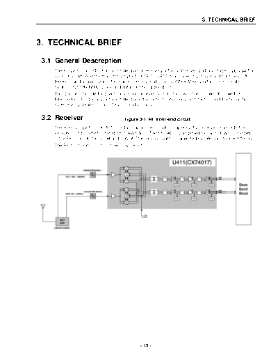
3.2 Receiver Figure 3-1. RF front-end circuit.
The Receiver part in CX74017 contains all active circuits completely, full receiver chain with the
exception of discrete front-end RF SAW filters. The filtered and amplified signal is down converted
in the RF-mixer to the baseband output. The receiver path is supported by internal channel filtering.
The RF front-end circuit is shown Figure 3-1.
- 13 -
3. TECHNICAL BRIEF
A. RF front end
RF front end consists of Antenna Switch(U405), dual band LNAs integrated in transceiver(U411).
The Received RF signals (GSM 925MHz ~ 960MHz, DCS 1805MHz ~ 1880MHz) are fed into the
antenna or mobile switch. An antenna matching circuit is between the antenna and the mobile
switch.
The Antenna Switch (U405) is used to control the Rx and TX paths. And, the input signals VC1 and
VC2 of a U405 are connected to 2-Input AND Gates(U401) to switch either TX or RX path on.
When the RX path is turned on, the received RF signal then feeds either Rx_900_RF or
RX_1800_RF path selected by GSM-RX and DCS-RX respectively. This Rx_900_RF path contains
one SAW filter, followed after the Antenna Switch (U405), to filter any unwanted signal apart from
the DCS RX band. And, the RX_1800_RF path is the same case.
The logic and current for Antenna Switch is given below Table 3-1.
Table 3-1. The logic and current
VC1 VC2 Current
GSM TX 0V 2.7 V 10.0 mA max
DCS TX 2.7 V 0V 10.0 mA max
GSM/DCS RX 0V 0V < 0.1 mA
These two paths are then connected to the LNAGSMN (#11) and LNADCSIN (#13) of CX74017
(U411), respectively. A low-noise bipolar RF amplifier, contained within the U411, amplifies the RF
signal. The RF signals from the front-end pass to the receiver mixers within the U411 device.
B. Demodulator and baseband processing
In direct conversion receiver there is only one mixer down-converting received RF signal to BB
signal directly. The gain down converting mixer is 40dB at high gain mode and 22dB at low gain
mode.
The Rx gain setting is done in the AGC algorithm. The nominal gain of the receiver is set as a
function of the expected signal strength at the antenna input so that a desired level is reached at
the Rx I/Q. 7 blocks in the receiver chain have variable gains, LNA, Mixer, LPF1, VGA1, gmC Filter,
Auxiliary gain control and VGA2. The gain settings can be adjustable via 3-wire bus control lines.
The baseband signals pass via integrated low-pass filters to the baseband A/D converters.
The remainder of the channel filtering is performed by the baseband chipset. The demodulator
contains switches to maintain the sense of the baseband I/Q outputs with respect to the incoming
RF signal on both GSM900 and DCS 1800.
C. DC Offset Compensation
Three correction loops ensure that DC offsets, generated in the CX74017, do not overload the
baseband chain at any point.
After compensation, the correction voltages are held on capacitors for the duration of the receive
slot(s). A rising edge on the RXEN signal, selected via the serial interface, placed the DC
compensation circuitry in the track mode.
- 14 -
3. TECHNICAL BRIEF
3.3 Transmitter Part
The Transmitter part contains CX74017 active parts and PAM, APC IC, coupler and Antenna
Switch. The CX74017 active part consists of a vector modulator and offset phase-locked loop
block(OPLL) including down-converter, phase detector, loop filter and dual band transmit VCO
which can operate at either final RF output frequency. The RF GMSK outputs from the transmit
VCO are fed directly to the RF power amplifiers.
TXIP
TXIN
Figure 3-2. Transmitter Block diagram
The peak output power and the profile of the transmitted burst are controlled by means of a closed
feedback loop. A dual band directional coupler is used to sample the RF output from either PA.
The PA outputs from the directional coupler pass to the antenna connector via Antenna Switch.
A. IF Modulator
The baseband converter(BBC) within the GSM chipset generates I and Q baseband signals for the
transmit vector modulator. The modulator provides more than 40dBc of carrier and unwanted side-
band rejection and produces a GMSK modulated signal. The baseband software is able to cancel
out differential DC offsets in the I/Q baseband signals caused by imperfections in the D/A
converters.
The TX-Modulator implements a quadrature modulator. The IF-frequency input signal is split into
two precise orthogonal carriers, which are multiplied by the baseband modulation signal IT/ITX and
QT/QTX. It is used as reference signal for the OPLL.
- 15 -
3. TECHNICAL BRIEF
B. OPLL
The offset mixer down converts the feedback Tx RF signal using LO to generate a IF modulating
signal. The IF signal goes via external passive bandpass filter to one port of the phase detector.
The other side of the phase detector input is LO signal. The phase detector generates an error
current proportional to the phase difference between the modulated signal from the offset mixer and
the reference signal from the LO.
The error current is filtered by a second order low-pass filter to generate an output voltage which
depends on the GMSK modulation and the desired channel frequency. This voltage controls the
transmit VCO such that the VCO output signal, centered on the correct RF channel, is frequency
modulated with the original GMSK data. The OPLL acts as a tracking narrowband band pass filter
tuned to the desired channel frequency. This reduces the wideband noise floor of the modulation
and up-conversion process and provides significant filtering of spurious products.
C. Synthesizer
The CX74017 includes a fully integrated UHF VCO with an on-chip LC tank.
A single sigma-delta fractional-N synthesizer can phase lock the local osillator used in both transmit
and receive path to a precision frequency reference input. Fractional-N operation offers low phase
noise and fast setting times, allowing for multiple slot applications such as GPRS.
The generated frequency is given by the following equation
=
where : f VCO = Generated VCO frequency
N = N-divider ratio integer part
FN = Fractional setting
R = R-divider ratio
f VCO = Reference Frequency
- 16 -
3. TECHNICAL BRIEF
The counter and mode settings of the synthesizer are also programmed via 3-wire interface.
f ref 13MHz
Figure 3-3. Synthesizer Block diagram
D. TX APC Part
The AD8315[U412] is a dual band RF power controller for RF power amplifiers operating in the
850MHz to 2GHz range.
The AD8315[U412] controls the power output of the selected RF channel. RF power is controlled by
driving the RF amplifier power control pins and sensing the resultant RF output power via a
directional coupler. The RF sense voltage is peak detected using an on-chip Schottky diode.
This detected voltage is compared to the DAC voltage at the VSET pin to control the output power.
An internal input signal[TXRAMP] is applied to the positive input of the AD8315 amplifier during the
TXEN mode and a directional coupler near the antenna feeds a portion of the RF output signal back
to the AD8315 peak detector converts this signal to a low frequency feedback signal that balances
the amplifier when this signal equals the RAMP input signal level.
E. Power Amplifier
The PF08107B[U409] is Dual band amplifier for E-GSM(880 to 915MHz) and DCS1800(1710 to
1785MHz). The efficiency of module is the 50% at nominal output power for E-GSM and the 43% at
32dBm for DCS1800. This module should be operated under the GSM burst pulse. To avoid
permanent degradation, CW operation should not be applied. To avoid the oscillation at no input
power, before the input is cut off, the control voltage Vapc should be control to less than 0.5V.
We have to improve thermal resistance, the through holes should be layouted as many as possible
on PCB under the module. And to get good stability, all the GND terminals and the metal cap should
be soldered to ground plane of PCB.
- 17 -
3. TECHNICAL BRIEF
3.4 13 MHz Clock
The 13 MHz clock (VC-TCXO-208C) consists of a TCXO (Temperature Compensated Crystal
Oscillator) which oscillates at a frequency of 13 MHz.
It is used within the CX74017 RF Main Chip, BB Analog chip-set (AD6521), and Digital (AD6522).
.
Figure 3-4. VCTCXO Circuit.
3.5 Power Supplies and Control Signals
There are two regulators used in the phone to provide RF power. One is contained inside of
ADP3408 (U101), power management IC to provide the power for the VCTXO (X302). The other is
used to provide the power for remaining RF circuits.
Table 3-2.
Regulator Voltage Powers Enable Signal
Regulator 1
2.7 V 0.5 V VCTXO
(U1, 2V7_VTCXO)
Regulator 2
2.85 V 0.5 V RF circuitry VSYNTHEN
(U414, RF2V8)
Figure 3-5. Regulator Circuit.
- 18 -
3. TECHNICAL BRIEF
3.6 Digital Main Processor
The AD6522 is an ADI designed processor.
Figure 3-6. Top level block diagram of the AD6522 internal architecture.
BUS Arbitration Subsystem
It is to work as a cross point for data accesses between the three main busses. EBUS is for external
accesses, primarily from Flash memory for code and data. RBUS is for internal RAM access. PBUS
is for access to internal peripheral modules such as UART, RTC or SIM. In addition to the three
main system busses, it has SBUS, IOBUS and DMABUS.
DSP subsystem
It consists of ADI DSP, Viterbi coprocessor, Ciphering unit and a cache memory/controller system.
The DSP can run at a maximum clock frequency of 78 MHz at 2.45 V. The Viterbi and ciphering
accelerators enable a very efficient implementation of the channel equalization, encryption and
decryption tasks.
- 19 -
3. TECHNICAL BRIEF
MCU subsystem
It consists of an ARM7TDMI central processing unit, a boot ROM, a clock generation and access
control module.
The maximum clock frequency for the ARM7TDMI is 39 MHz at 2.45 V.
The main clock is 13MHz and it is provided by VCTCXO. The Clock & BS(Bus Select) generator
make internal clock by multiplying the main clock by 1X, 1.5X, 2X and 3X.
The boot ROM contains MCU code for basic communication between the ARM and one of the serial
ports in the Universal System Connector subsystem.
Peripheral subsystem
It contains four major groups of elements.
The MMI group is a collection of all the functionality that are needed to implement a complete user
interface including keyboard, display, backlight, RTC, general purpose I/O etc.
House Keeping group consists of three different sub-modules: The Watch Dog Timer, the Interrupt
Controller, and the general timers.
GSM system group consists of the time base generation together with the synthesizer interface,
which form the radio control.
Direct Memory Access is located between the three system buses (PBUS, RBUS and EBUS) and
can move any data from any address location on one system bus to any address location on
another system bus.
- 20 -
3. TECHNICAL BRIEF
Figure 3-7. System interconnection of AD6522 external interfaces
- 21 -
3. TECHNICAL BRIEF
Interconnection with external devices
RTC block interface
Countered by external X-TAL
The X-TAL oscillates 32.768KHz
LCD module interface
Controlled by LCD_MAIN/SUB_CS, LCD_RES, LCD_A0, /WR, /RD, DATA [00...07] ports
Table 3-3.
Description
LCD_MAIN_CS
LCD chip enable. Each LCD has CS pin
LCD_SUB_CS
LCD_RES This pin resets LCD module.
This pin determines whether the data to LCD module is display data or
LCD_A0
control data
/WR, /RD Read/Write control
DATA [00...07] Parallel data line
RF interface
The AD6522 control RF parts through TXEN, RXON1, RXON2, AGCEN, SDATA, SCLK, SEN etc.
Table 3-4.
Signal Name Description
TXEN TX Enable/Disable
RXON1 LNA, Mixer1 On/Off
RXON2 Mixer 2 On/Off
AGCEN AGC Enable/Disable
SDATA Serial Data to PLL
SCLK Clock to PLL
SEN PLL Enable/Disable
- 22 -
3. TECHNICAL BRIEF
SIM interface
The AD6522 check status periodically in call mode if SIM card is inserted or not, but the AD6522
don't check in deep sleep mode.
Interface by SIM_IO, SIM_CLK, SIM_RST
Table 3-5.
Description
This pin receives and sends data to SIM card. G5200 support only 3.0
SIM_IO
volt interface SIM card.
SIM_CLK Clock 3.5MHz frequency.
SIM_RST Reset SIM block.
Figure 3-8.
Key interface
Include 5 column and 5 row
The AD6522 detect key press by interrupt
ADP3408 interrupt
There are two interrupts EOC and CHARGEDETECT
EOC: End of Charge. Charging would be stopped when AD6522 receive this input.
CHARGEDETECT: This interrupt is generated when charge is inserted.
- 23 -
3. TECHNICAL BRIEF
3.7 Analog Main Processor
AD6521
Figure 3-9. AD6521 function block diagram
- 24 -
3. TECHNICAL BRIEF
BB Transmit section
This section generates in-phase and quadrature BB modulated GMSK signals (BT = 0.3) in
accordance with GSM 05.05 Phase 2 specifications
The transmit channel consists of a digital GMSK modulator, a matched pair of 10-bit DACs and a
matched pair of reconstruction filter
BB Receive section
This section consists of two identical ADC channels that process baseband in-phase(I) and
quadrature(Q) input signals.
Each channel consists of a coarse switched capacitor input filter, followed by a high-order sigma-
delta modulator and a lowpass digital filter
Auxiliary section
This section contains two auxiliary DACs(AFC DAC, IDAC) for system control.
This section also contains AUX ADC and Voltage Reference
AUX ADC: 6 channel 10 bits
AFC DAC: 13 bits
IDAC: 10 bits
Voiceband section
Receive audio signal from MIC. G5200 use differential configuration.
Send audio signal to Receiver. G5200 use differential configuration.
It interconnect with external device like main microphone, main receiver, ear-phone and Hands free
kit
through the VINNORP, VINNORN, VOUTNORP, VOUTNORN, VINAUXP, VINAUXN,
VOUTAUXP, VOUTAUXN
VINNORP, VINNORN: Main MIC positive/negative terminal.
VOUTNORP, VOUTNORN: Main Receiver positive/negative terminal.
VINAUXP, VINAUXN: Hands free kit mic positive/negative terminal.
VOUTAUXP, VOUTAUXON: Hands free kit speaker positive/negative terminal.
- 25 -
3. TECHNICAL BRIEF
3.8 Power Management
ADP3408
Figure 3-10. ADP3408 inner block diagram.
Power up sequence logic
The ADP3408 controls power on sequence
Power on sequence
If a battery is inserted, the battery powers the 6 LDOs.
Then if PWRONKEY is detected, the LDOs output turn on.
REFOUT is also enabled
Reset is generated and send to the AD6522
- 26 -
3. TECHNICAL BRIEF
LDO block
There are 6 LDOs in the ADP3408
Table 3-6.
Description
VSIM 2.86 V (is provided to SIM card)
VCORE 2.45 V (is provided to the AD6522 & AD6521's digital core)
VRTC 2.45 V (is provided to the RTC and Backup Battery)
VAN 2.45 V (is provided to the AD6521 I/O and used as microphone bias)
VTCXO 2.715 V (is provided to VCTCXO)
VMEM 2.80 V (is provided to Flash)
Battery charging block
It can be used to charge Lithium Ion and/or Nickel Metal Hydride batteries. G5200 use Li-Ion battery
only. Charger initialization, trickle charging, and Li-Ion charging control are implemented in
hardware.
Charging Process
Check charger is inserted or not
If ADP3408 detects that Charger is inserted, the CC-CV charging starts.
Exception: When battery voltage is lower than 3.2V, the precharge (low current charge mode) starts
firstly.
And the battery voltage reach to 3.2V the CC-CV charging starts.
Pins used for charging
CHARGERDETECT: Interrupt to AD6522 when charger is plugged.
CHARGEEN: Control signal from AD6522 to charge Li+ battery
EOC: Interrupt to AD6522 when battery is fully charged
GATEIN: Control signal from AD6522 to charge NiMH battery. But, not used.
MVBAT: Battery voltage divider. Divide ratio is 1:2.3 and it is sensed in AD6521 AUX_ADC
TA (Travel Adaptor)
Input voltage: AC 85V ~ 260V, 50~60Hz
Output voltage: DC 5.2V ( ◦ Jabse Service Manual Search 2024 ◦ Jabse Pravopis ◦ onTap.bg ◦ Other service manual resources online : Fixya ◦ eServiceinfo