Service Manuals, User Guides, Schematic Diagrams or docs for : LG Mobile Phone LG G8000 LG G8000 8
<< Back | HomeMost service manuals and schematics are PDF files, so You will need Adobre Acrobat Reader to view : Acrobat Download Some of the files are DjVu format. Readers and resources available here : DjVu Resources
For the compressed files, most common are zip and rar. Please, extract files with Your favorite compression software ( WinZip, WinRAR ... ) before viewing. If a document has multiple parts, You should download all, before extracting.
Good luck. Repair on Your own risk. Make sure You know what You are doing.
Image preview - the first page of the document
>> Download LG G8000 8 documenatation <<
Text preview - extract from the document
3. TECHNICAL BRIEF
3. TECHNICAL BRIEF
3.1 Receiver
The receiver part consists of a dual band (GSM & DCS) antenna switch, two RF SAW filters, an
external dual RF VCO and a transceiver IC (TRF6150). All active circuits for a complete receiver
chain with the exception of RF VCO are contained in the transceiver IC (TRF6150).
The TRF6150 chip set has direct conversion structure, so the received RF signal is directly
converted to base band I and Q signal by the transceiver IC (IF frequency is 0 Hz), which contains
two LNAs and three direct conversion demodulators for E-GSM, DCS and PCS. The demodulated I
and Q signals pass two base band AGC amplifiers and a channel filter, which are on both I and Q
signal paths. The RF front-end circuit is shown Figure 3-1.
Figure 3-1. RF front-end circuit
- 12 -
3. TECHNICAL BRIEF
3.1.1 RF front end
RF front end consists of an antenna, a dual band antenna switch, two RF SAWs and two LNAs for E-
GSM, DCS band, which are contained in the transceiver IC (TRF6150).
The RF received signals (GSM 925MHz ~ 960MHz, DCS 1805MHz ~ 1880MHz) are input via the
antenna or coaxial connector. An antenna matching circuit is between the antenna and the
connector.
The antenna switch (FL103) is used to control the Rx and TX paths, which has two control signals
VC1 and VC2 that are connected to 4-Input NOR Gate (U102) to switch either TX or RX path on.
When the RX path is turned on, the received RF signal, which has passed through the dual band
antenna switch, is filtered by an appropriate RF SAW filter for better stop band rejection. The filtered
RF signal is amplified by an LNA integrated in the transceiver IC(TRF6150) and pass to a direct
conversion demodulator. This process is the same both GSM and DCS.
The logic and current is given below. Table 3-1.
Table 3-1. The logic and current
VC1 VC2
GSM TX 2.7 V 0V
DCS TX 0V 2.7 V
GSM/DCS RX 0V 0V
3.1.2 Demodulator and Baseband Processing
IF stage is not necessary in this system because the receiver is based on direct conversion
architecture. So the RX LO frequency is the same as input radio frequency. The amplified signal at
LNA stage passes to a direct conversion demodulator and is mixed down to generate I&Q BB
signals. The BB I&Q signals pass via two integrated baseband amplifiers with digitally programmable
gain and two fully integrated baseband channel filters to the baseband A/D converters which is
contained in baseband chipset. Figure 3-2 shows RX path block diagram.
3.1.3 DC offset compensation
The transceiver IC(TRF6150) is based on direct-conversion architecture. This implies that a parasitic
DC offset may appear at the output of the IQ demodulator. To reduce the static offset due to
components mismatch and LO self-mixing, the IC includes a hardware DC offset compensation
circuit on both I and Q base band paths. The transceiver IC uses a divider by 2 for LO generation in
EGSM and a multiplier by 2 in DCS to minimize the DC offset generated by self mixing and the LO
radiation. In addition, a quadrature demodulator gain mismatch calibration system is used to reduce
the signal distortion.
- 13 -
3. TECHNICAL BRIEF
Figure 3-2. RX path block diagram
Table 3-2. Gain and Noise Figure of RX path
Ant. switch RF SAW Filter I,Q demodulator (LNA+Mixer)
GSM -0.6 -2.5 26
Gain(dB)
DCS -0.7 -2.4 23
GSM 3
NF(dB)
DCS 3.5
Table 3-3. Total Gain and Noise Figure of RX path
Total Gain Total Noise Figure
GSM, EGSM 22.9 dB 7.2 dB
DCS 19.9 dB 7.4 dB
- 14 -
3. TECHNICAL BRIEF
3.2 Synthesizer
The TRF6150 includes two synthesizer parts. Two synthesizers consist of an IF synthesizer, which is
an integer-N synthesizer, and a RF synthesizer, which is a fractional-N synthesizer. The TRF6150 is
a transceiver IC suitable for GSM and DCS GPRS up to class 12 applications. So, synthesizers use
a number of techniques to improve lock time, making them well suited to GPRS.
The main fractional-N synthesizer (RF synthesizer), which includes a RF VCO with external tank
circuits, is necessary for both transmitting and receiving operation. The RF VCO works only when
the transmitting operation is on. The main fractional-N synthesizer has frequency band from 1294
MHz to 1356 MHz. Output frequency of the RF VCO is set by the factional number, prescaler and
counter. A buffer amplifier follows the RF VCO. The purpose of the buffer is to give reverse isolation
and prevent any frequency pulling of the VCO when the transceiver is powered UP and DOWN.
A dual band external VCO, which uses the PLL block of the main fractional-N synthesizer, is
necessary for transmitting and receiving operation. The dual band means that it can support GSM,
DCS frequency operation. For transmitting operation, the OPLL block of the TRF6150 directly
modulates the dual band external VCO with I and Q signals. For receiving operation, the external
VCO output frequency band is from 902 to 940MHz for DCS Rx and from 1850 to 1920MHz for GSM
Rx. The frequency of the signal from the external VCO is divided by 2 for GSM Rx and is doubled by
2 for DCS Rx operation before entering into the direct conversion mixer.
The auxiliary integer-N synthesizer (IF synthesizer), which includes an IF VCO with external tank
circuits, is necessary for transmitting operation only. The IF VCO has a frequency band from 832
MHz to 858 MHz. Output frequency of IF VCO is settled by prescaler and counter. The fractional
counter in the RF synthesizer just differs from the IF synthesizer. The IF VCO is also followed by a
buffer amplifier, which is to give reverse isolation and prevent any frequency pulling of the VCO
when the transceiver is powered UP and DOWN.
A fixed reference frequency of 1.3MHz for Rx (or 2.6MHz for Tx) is generated by a reference divider
from the external applied 13 MHz crystal oscillator.
The phase frequency detector with charge pump provides programmable output current, which could
drive the capability and the pulse width.
The counter and mode settings of the synthesizer in the TRF6150 are programmed via 3-wire
interface.
Table 3-4. 3-wire BUS of Synthesizer in the TRF6150
Pin Number Description
TSPCLK 11 Serial clock input to the synthesizer
TSPDATA 12 Serial data input to the synthesizer
TSPEN 13 Input latches the serial data transferred to the synthesizer
- 15 -
3. TECHNICAL BRIEF
Dual band VCO :
902 ~ 940MHz DCS Rx
1850 ~ 1920MHz GSM Rx
RF SYNTHESIZER
2.6/1.3MHz
13MHz
or :2 : 5/ 10
26MHz PFD
1294 ~ 1356MHz
TANK
RX : OPEN
7 bits 4 bits 4 bits 16/17
TX : CLOSED A B FN P/P+ 1
2.6MHz
IF SYNTHESIZER
Delay
PFD
6 bits 3bits 8/9
A B P/P+ 1 TANK
832 ~ 858MHz
Figure 3-3. Synthesizer internal Block Diagram
- 16 -
3. TECHNICAL BRIEF
The IF and RF output frequencies of the TRF6150 are set by programming the internal divider registers.
The frequency setting equations of the IF and RF frequencies are as follows.
is the output frequency of the IF VCO (the auxiliary integer-N synthesizer) and fRFout is the output
frequency of the RF VCO (the main fractional-N synthesizer). The frequency band of the RF VCO is from
1294MHz to 1356 MHz, and the frequency band of the IF VCO is from 832MHz to 858Mhz, which
frequency bands are only for the transmitting operation.
C116
VT 13
FL101 R107
C118
ENFVF382S18
C117 R109
57 MAINSPUP2
R110
R111
59 TXRXCP
58 R2
60
MAINSPUP14
MAINCP 5
MAIN PFD
PLL
U105
TRF 6150
R124
Interface
CLK 11
Serial
TSPCLK
R123 DATA 12
TSPDATA
TSPEN R128 EN 13
35MAINVCO
AUXCP 14
AFC C146 AUX.
R131 CRF 16 PLL
X101
VCC7 22
AUXVCOP 23
AUXVCON 24
C175 D102 C156
C142 VC-TCXO-208C
HVC369B
R140
C164 L108
C167
L105
C174
R145 C185
C176 C177
R141 L109 C184
R139
R142 R143
C178 L110
R137 C183
C179
D103
SMV 1233-074
Figure 3-4. Synthesizer circuit
- 17 -
3. TECHNICAL BRIEF
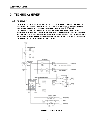
3.3 Transmitter
The Transmitter part contains TRF6150 active parts, PAM, coupler, dual schottky diode and dual
band VCO. The TRF6150 active parts consist of the vector modulator and offset phase-locked loop
block (OPLL) including down-converter, phase detector, and APC IC for power control. The VCO
feed the output frequencies into PAM and TRF6150 for Tx local frequency. The peak output power
of the PAM is controlled by means of a closed feedback loop. A dual band directional coupler is
used to control the RF output from the PAM. The PAM outputs from the directional coupler pass to
the antenna connector via an integrated dual band antenna switch module.
2.6/1.3MHZ
RFout_rx = (P*A + B + FN/13)*1.3MHz
MAINspup1
TX
LF MAINcp
:5/10 :2 CRF
RX
1294~1356 MHz
TANK MAINvco
VC1 VC2
VC1
TX 2.6V 0V
GSM
VC2
RX 0V 0V 16/17 4bits 4bits 7bits VR4in
DCS
TX 0V 2.6V P/P+1 FN B A CLK
RX 0V 0V Serial Control DATA
Logic & EN
Resisters
RESETZ
AUXcp Delay
LF
SHS-M090B
832~858 MHz
AUXvcon
TANK 8/9 3bits 6bits
AUXvcop
P/P+1 B A
DCS EGSM
APC DAC
IFout = (P*A + B)*13MHz
APCEN PA
DETD CONTROLLER RFout_tx = (P*A + B + FN/13)*2.6MHz
DETR
Vapc FILT
/2
BAT15-05W
OMIXrf
416-429MHz
LBTX
R3
IN
LF TXRXcp
PFD IP
MAINspup2
HBTX 90◦ Jabse Service Manual Search 2024 ◦ Jabse Pravopis ◦ onTap.bg ◦ Other service manual resources online : Fixya ◦ eServiceinfo