Service Manuals, User Guides, Schematic Diagrams or docs for : LG TV lg_we32q10ip__mc993a__266

<< Back | Home

Most service manuals and schematics are PDF files, so You will need Adobre Acrobat Reader to view : Acrobat Download Some of the files are DjVu format. Readers and resources available here : DjVu Resources
For the compressed files, most common are zip and rar. Please, extract files with Your favorite compression software ( WinZip, WinRAR ... ) before viewing. If a document has multiple parts, You should download all, before extracting.
Good luck. Repair on Your own risk. Make sure You know what You are doing.


Image preview - the first page of the document
lg_we32q10ip__mc993a__266


>> Download lg_we32q10ip__mc993a__266 documenatation <<

Text preview - extract from the document
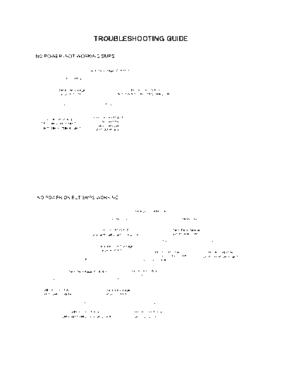
                                 TROUBLESHOOTING GUIDE


                                             C834


               R857
D805, D803, ZD804, Q801


                                                                 3


                             Q04,Q851,Q852,Q853,IC802,IC804                           41


                                        8   IC507
                                                                     IC01,IC301,FR440,FR441,   D406,FR436,Q804,Q805.
                          8.0V                                       D407,D408.


                                                        IC507.
                                            75V


R405, D811, FR848.

                                                                 135V


           D813,R811,R812,T403,Q402,L801.            Q401, Q402, T401.
FR459, FR901.


                             61


     20~25, 28~29


                     10~17        IC503.               Q205, IC201.


 IC503.                 29~30, 32~37        IC504.


                                           Check the waveform
                    IC504.                 at pin 54~61 of IC507.


                                                       Check/Replace IC507,
                Check/Replace IC507.
                                                           Q502~Q510.
                           1, 6     IC301.


  FR440,FR441,D407,D408.                     19, 20   IC507.


                     IC507, Q501, Q514.                  IC301, D301.


PIN CUSHION

                       21         IC507.


       IC507.                                    IC401


                           IC401                         R424.


                                     Q404, Q405.                        D402.
                   12   IC701.


                                      2.4V


  IC701, X701.                    6


                   Q701.                     35,36,37   IC507.


                                                          IC507.


          Check the waveform
           at pin 9 of P504B.

                                      NORMAL

                           Check/Replace Q2001~Q2003,
IC507,Q511~Q513.              IC2001,D2008~D2009.


                                                  31V


    FR852, D814.
FR848,D811,FR829,ZD103.


                                        IC102, R110 .


                          61


                               19
                                    IC201,Q203,Q204,IC204.


          IC03
NO VGA
                    Check the waveform
                    at pin 52, 60 of IC501.
        NO                                    NORMAL


Check/Replace                          Check the waveform
   VGA01.                           at pin 31, 32, 33 of IC507.

                           NO                       NORMAL


                 Check/Replace                Check/Replace
                    VGA01.                       IC507.


NO COMPONENT
                     Check the voltage
                     at pin 44 of IC01.
        0V                                    5V


Check/Replace                         Check the waveform
    IC01.                             at pin 10~13 of IC203.

                           NO                       NORMAL


             Check the waveform               Check/Replace
             at pin 6~8 of IC203.                IC503.

                     NO                             NORMAL


                 Check/Replace                Check/Replace
                Q202, Q208, Q209.                IC203.
                                                ADJUSTMENT INSTRUCTIONS
Y Safety Precautions                                                                          : SECAM-L' Adjustment
   1. It is safe to adjust after using insulating transformer between
      the power supply line and chassis input to prevent the risk of                            NOTE : This adjustment should be performed after PIF
      electric shock and protect the instrument.                                                       adjustment.
   2. Never disconnect leads while the TV receiver is on.
   3. Don't short any portion of circuits while power is on.                                     Test Point     : TP1
   4. The adjustment must be done by the correct appliances.
   5. Unless otherwise noted, set the line voltage to 230Vac!10%,                                Adjust         : VR102
      50Hz.
                                                                                                1) Turn on S1 and S3 and off S2.
Y Test Equipment required                                                                       2) Adjust VR102 so that the DC voltage may be indicated
   1.    RF signal generator (with pattern generator)
                                                                                                   2.5!0.1Vdc.
   2.    DC Power Supply
   3.    Multimeter (volt meter)
   4.    Oscilloscope
   5.    Color analyzer
                                                                                              : RF AGC (Automatic Gain Control) Adjustment

                        Main Board(Component side view)                                          Test Point     : J209 or Observing Display

                                                                                                 Adjust         : VR101
                           V    Multimeter or Oscilloscope

                                                     1                                          The RF AGC control (VR101) was aligned at the time of
                                         IC101                                                  manufacture for optimum performance over a wide range
Power-       JP7 IC05
                                        TDA4474
Supply                                                                                          conditions. Readjustment of VR101 should not be necessary
             JP4 IC102    TP1           24                            Signal-
  5V                                                         0.01pF   Generator                 unless unusual local conditions exist, such as ;
                5V                                7 JP1               38.9MHz (B/G,D/K,I,L)
                           L107
                                                 11 JP2               34.25MHz (SECAM-L')       1) Channel interference in a CATV system.
                4.7k


◦ Jabse Service Manual Search 2024 ◦ Jabse PravopisonTap.bg ◦ Other service manual resources online : FixyaeServiceinfo