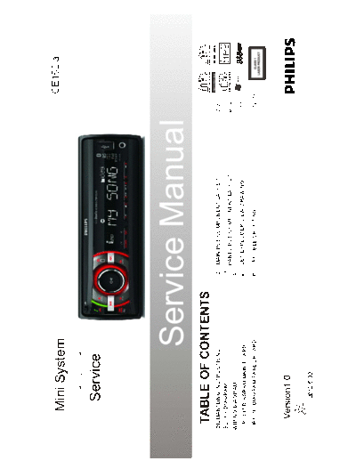
Service Manuals, User Guides, Schematic Diagrams or docs for : Philips Car Audio CE152 CE152
<< Back | HomeMost service manuals and schematics are PDF files, so You will need Adobre Acrobat Reader to view : Acrobat Download Some of the files are DjVu format. Readers and resources available here : DjVu Resources
For the compressed files, most common are zip and rar. Please, extract files with Your favorite compression software ( WinZip, WinRAR ... ) before viewing. If a document has multiple parts, You should download all, before extracting.
Good luck. Repair on Your own risk. Make sure You know what You are doing.
Image preview - the first page of the document
>> Download CE152 documenatation <<
Text preview - extract from the document
                                                                                                                                                                                CE152/all


DISMANTLING INSTRUCTIONS.................................................2               MAIN PCB COMPONENT LAYOUT............................................7-8
BLOCK DIAGRAM........................................................................3
                                                                                         PANEL PCB COMPONENT LAYOUT.........................................9-10
WIRING DIAGRAM......................................................................4
CIRCUIT DIAGRAM MAIN BOARD.............................................5                 SET EXPLODER VIEW DRAWING................................................11

CIRCUIT DIAGRAM PANEL BOARD..........................................6                   TROUBLE SHOOTING...................................................................12-13


                 2012-5-30
       The procedure of disassembling the unit
1. Remove A, B screws in the back cover as below picture showed; Use tweezer to prize up top cover as the blue arrow direction which showed as below picture and remove the
top cover then unplug the 2P microphone wire

                   A


               B


2.) Remove the four screws in C,D,E,F position in the heat sink, then remove the G screw in left side of the unit and the H, I screws which were for fixing the main board; remove the
main board

 C                                           E                                                                              I
                                                                                G
                                                                                                     H
 D                                           F


       The procedure of disassembling the panel
3
Wiring Diagram


           4
CIRCUIT DIAGRAM -MAIN BOARD


                  5
    39R


    39R


          M1/PAU                 MENU
          SW912                  SW901


                    180R
                                           180R
           M2/INT                 T-DN


                    R921
                                           R911
          SW913                  SW902


                    220R
                                           220R
          M3/RPT                EQ/AUDIO


                    R922
                                           R912
          SW914                  SW903


                    330R
                                           330R

                           MAX/SOUND/DBB
          M4/RDM


                    R923
                                           R913


          SW915                  SW904


                    470R
                                           470R


                                 T-UP
           M5/ST
                    R924
                                           R914


          SW916                  SW905


6
                    680R
                                           680R


          M6/PROG                BAND
                    R925
                                           R915


          SW917                  SW906
                    1K
                                           1K
                                                  CIRCUIT DIAGRAM -PANEL BOARD


                    R926
                                           R916


                                SOURCE
                                 SW907
                                           1K5


                                RETURN
                                 SW908
                                           2K2
                                           R918


                                   DISP
                                  SW909
                                           3K3


                                  ZONE
                                           R919


                                  SW910
PCB LAYOUT-MAIN BOARD TOP SIDE VIEW


                         7
PCB LAYOUT-MAIN BOARD BOTTOM SIDE VIEW


                     8
PCB LAYOUT-PANEL BOARD TOP SIDE VIEW


                          9
PCB LAYOUT-PANEL BOARD BOTTOM SIDE VIEW


                           10
SET EXPLODER VIEW DRAWING


                 11
Product Model        CE152                                                                  Date                          2012-5-28
       failure
NO. phenomena                                                              failure cause                                                             remark

                 a. To check whether the CN501(ISO) connector of the tail of the unit is connect well , Whether it is loose of the 15A fuse of the
                 ISO, or insert non in place.

              b. To check whether there is any contamination and bad contact on the 22Pin male/female connector on the panel and main
 1   NO Power board.
                 c. To check the U602 of voltage regulator IC,the output pin should be +3V3        the input pin should be +11V0.
                 d. At the unit ACC ON, To check the 36 pin voltage of the U201(MCU) should be low level .
                 e. To check the oscillation frequence of crystal CF202 shuold be 32.768KHz .

                 a.To check whether there is any contamination and bad contact on the 22Pin male/female connector of the panel and main
                 board. If necessary, can exchange the panel to test whether the defective is occurred by the unit or panel.
       LCD
 2
     abnormal b.To Check the voltage of the 56 pin of the IC901(75823) ,should be +5V0.

                 c.To check the voltage of the L303 of the MAIN board,should be +5V0.
                 a. To check whether the volume knob is turn to the minimum position.
                 b. To check whether the unit is at MUTE mode, press SOURCE button and check whether it is effective of the input sound
                 source.
       NO
 3    audio      c. To check whether the connection of audio output wire of ISO connector is correct; wrong connection or short circuit to the
      output     ground will caused the protection of the power amplifier( no voltage output).

                 d . To check the circuit of power amplifier U501(7388 IC) and VOLUME U301(7313 IC).
                 e. To check the voltage of 22 PIN(MUTE) of power amplifier U501(7388 IC) , normally should be +4V0.
                 a. To check the antenna of the AM/FM tuner.
                 b. To check whether the strength of then input signal of the tuner is too weak.
 4
                 c. To check the voltage of the 12 pin   13 pin of the U131 of the tuner IC, should be +3V3.
                 d. To check the oscillation frequence of crystal XL130 of the tuner IC,shuold be 32.768MHz


                                                                                12
         failure
NO.                                                                         failure cause                                                  remark
       phenomena
                      a. To check whether the USB/SD signal format is correspond to the request of the unit.

                      b. To check the voltage of the the uppermost pin of the USB connector, should be +5V0.

 5    USB defective c. To check whether there is any wearing and scratch of the shrapnel and pin of the panel USB.

                      d.To check whether there is any contamination and bad contact on the 22Pin male/female connector of the panel and
                      main board. If necessary, can exchange the panel to test whether the defective is occurred by the unit or panel.

                      a. To check the SOURCE shoule be in MP3-LINK mode.

                      b. To check the MP3-LINK input signal.
 6    AUX defective
                      c. To check whether there is any contamination and bad contact on the 22Pin male/female connector of the panel and
                      main board. If necessary, can exchange the panel to test whether the defective is occurred by the unit or panel.


                      a   Check the unit should be in pair with the BT phone connection status.

 7    BT defective b      To Check the MIC connector CN801 whether there is poor contact. or insert non in place.

                      c   To check the 4 pin of the BT module,should be +5V0.


                                                                            13
◦ Jabse Service Manual Search 2024 ◦ Jabse Pravopis ◦ onTap.bg ◦ Other service manual resources online : Fixya ◦ eServiceinfo