Service Manuals, User Guides, Schematic Diagrams or docs for : Philips Audio HTS5120 HTS512012_SB-EX-SI_1308652010
<< Back | HomeMost service manuals and schematics are PDF files, so You will need Adobre Acrobat Reader to view : Acrobat Download Some of the files are DjVu format. Readers and resources available here : DjVu Resources
For the compressed files, most common are zip and rar. Please, extract files with Your favorite compression software ( WinZip, WinRAR ... ) before viewing. If a document has multiple parts, You should download all, before extracting.
Good luck. Repair on Your own risk. Make sure You know what You are doing.
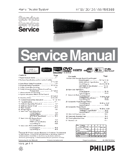
Image preview - the first page of the document
>> Download HTS512012_SB-EX-SI_1308652010 documenatation <<
Text preview - extract from the document
Home Theater System                                                                                    HTS5120/12/51/55/78/93/98


                 CLASS 1
              LASER PRODUCT


Contents                                                         Page                                                                                      Page
                                                                                        Contents
1 Repair Scenario Matrix ...............................................1-1        19 Main Unit--Decoder Board Circuit Diagram
2 Technical Specification and Connection Facilities                                                    Circuit Diagram ...................... 15-7 to 15-10
                 .................................................. 2-1 to 2-3                         EN29LV320A IC Specification ..........15-11
3 Laser Beam Safety Precautions..................................3-1                                   Circuit Diagram ...................... 15-12 to 15-15
4 Important Safety Precautions ......................... 4-1 to 4-2                                    UDA1355H IC Specification ............ 15-16
5 Safety Check After Servicing .................................... 5-1                                Layout Diagram ................................ 15-17
6 Safety Information General Notes & Lead Free                                     20 Main Unit--AMP Board
                  Requirement ............................ 6-1 to 6-2                                   Circuit Diagram .................................. 15-18
7 Standard Notes For Servicing .................................. .7-1                                  Layout Diagram ................................. 15-19
8 Special Information BGA IC & Flat Pack-IC                                        21 Main Unit--Radio Transmit Board
                ................................................... 8-1 to 8-3                          Circuit Diagram ...................... 15-20 to 15-22
9 Direction of Use ...............................................9-1 to 9-5                            CC2400 IC Specification .................. 15-23
10 Cabinet Disassembly Instructions ................... 10-1 to 10-2                                    Layout Diagram ................................. 15-24
11 Troubleshooting ..................................................... 11-1      22 Subwoofer--Radio Receiver Board
12 Software Upgrading Procedure ............................. 12-1                                       Circuit Diagram ..................... 15-25 to 15-27
13 Software Version Check ........................................ 12-2                                 Layout Diagram ................................. 15-28
                                                                                   23 Subwoofer--Power Board
14 Block Diagram ........................................................13-1
15 Wiring Diagram ...................................................... 14-1                           Circuit Diagram ..................... 15-29 to 15-30
                                                                                                         TDA8920 IC Specification ................ 15-31
16 Main Unit--Touch Button Board
                                                                                                        Layout Diagram ................................. 15-32
                  Circuit Diagram ................................. 15-1
                  Layout Diagram ................................ 15-1             24 Main Unit Exploded View ............................................ 16-1
                 WT5700 IC Specification ................. 15-2                    25 Subwoofer Exploded View ...........................................16-2
17 Main Unit--VFD Display Board                                                    26 Packing Exploded View ...............................................16-3
                 Circuit Diagram ................................. 15-3            27 Revision List ................................................................17-1
                 PT6311 IC Specification ................... 15-4
                  Layout Diagram ................................ 15-5
18 Main Unit-- IPOD,USB & MP3 Board                                                                            Feature
                                                                                                                  Different /12 /51 /55 /78 /93 /98
                Circuit Diagram ................................. 15-6                                 Features
                 Layout Diagram ................................ 15-6
                                                                                                         RDS
◦ Jabse Service Manual Search 2024 ◦ Jabse Pravopis ◦ onTap.bg ◦ Other service manual resources online : Fixya ◦ eServiceinfo