Service Manuals, User Guides, Schematic Diagrams or docs for : Philips DVD-Video HDRW720-69 Philips-HDRW720-69 dvd video recorder DVD Service Manual,Circuit diagram,User's Manual
<< Back | HomeMost service manuals and schematics are PDF files, so You will need Adobre Acrobat Reader to view : Acrobat Download Some of the files are DjVu format. Readers and resources available here : DjVu Resources
For the compressed files, most common are zip and rar. Please, extract files with Your favorite compression software ( WinZip, WinRAR ... ) before viewing. If a document has multiple parts, You should download all, before extracting.
Good luck. Repair on Your own risk. Make sure You know what You are doing.
Image preview - the first page of the document
>> Download Philips-HDRW720-69 dvd video recorder DVD Service Manual,Circuit diagram,User's Manual documenatation <<
Text preview - extract from the document
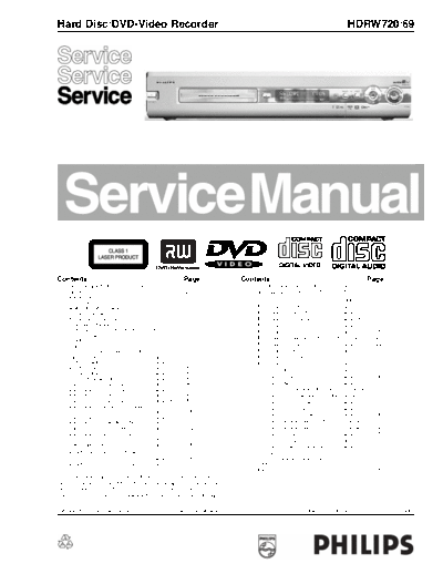
Hard Disc/DVD-Video Recorder                                                                                                      HDRW720/69


Contents                                                   Page                   Contents                                                  Page
1   Technical Specifications and Connection                                            In / Out Extension Board (IOE)        (Diagram 12)    113.
    Facilities                                              2                          DB Chrysalis F: IDE, UARTS, RESET, BE
    Diversity Matrix                                        2
    PCB Locations                                           5                                                        (Diagram 1)             115
2   Safety Information, General Notes                       6                         DB Chrysalis F: 1394                (Diagram 2)        116
3   Directions for Use                                      8                         DB Chrysalis F: Audio PLL           (Diagram 3)        117
4   Mechanical Instructions                                 38                        DB Chrysalis F: Chrysalis           (Diagram 4)        118
5   Diagnostic Software                                     41                        DB Chrysalis F: 1.8V Power          (Diagram 5)        119
6   Block Diagrams, Waveforms, Wiring Diagram               79                        DB Chrysalis F: Prog. scan DAC      (Diagram 6)        120
    Wiring Diagram                                          79
                                                                                      DB Chrysalis F: Flash SDRAM EEPROM(Diagram 7)          121
    Waveforms                                               82
    Testpoints                                              85                        DB Chrysalis F: Video IO            (Diagram 8)        122
7   Circuit Diagrams and PWB Layouts                        88                        DB Chrysalis F: VIPs                (Diagram 9)        123
    Display Panel                         (Diagram 1)       88                        DB Chrysalis F: Faroudja            (Diagram 10)       124
    Front Connector (FC)                  (Diagram 2)       89                        DB Chrysalis F: IDE 2               (Diagram 11)       125
    Standby Panel (STBY)                  (Diagram 3)       93                        EPG Board: MCU                      (Diagram 1)        129
    Tray Left Panel (TRL)                 (Diagram 4)       94
    Tray Right Panel (TRR)                (Diagram 5)       95                        EPG Board: GSA03                    (Diagram 2)        130
    Analog Board:Fronted Video (FV)       (Diagram 1)       96                        EPG Board: Memory                   (Diagram 3)        131
    Analog Board: In / Out Video (IOV)    (Diagram 2)       97                        EPG Board: Sync Separator for System (Diagram 4)       132
    Analog Board: In / Out Audio (IOA)    (Diagram 3)       98                        EPG Board: C-Sync Separator for data (Diagram 5)       133
    Analog Board: Power Supply (PS)       (Diagram 4)       99                        EPG Board: PIP Controller           (Diagram 6)        134
    Analog Board: Multi Sound Processing (MSP)                                        EPG Board: Sync Adder for Y         (Diagram 7)        135
                                          (Diagram 5)       100
    Analog Board: VPS                     (Diagram 6)       101                       EPG Board: Colour Encoder           (Diagram 8)        136
    Analog Board: Follow Me (FOME)        (Diagram 7)       101                       EPG Board: An. switches for CVBS, Y, C (Diagram 9)     137
    Analog Board: Digital In/Out (DIGIO) (Diagram 8)        102                       EPG Board: An. switches for YUV,YPbPr (Diagram 10)     138
    Analog Board: Audio Converter (DAC_ADC)                                           EPG Board: Connectors               (Diagram 11)       139
                                          (Diagram 9)       103                       EPG Board: IIC Expander             (Diagram 12)       140
    Power Supply Interface (PSI)          (Diagram 10)      108                       EPG Board: Power Conversions        (Diagram 13)       141
    UP Sub Board: Central Controler (CECO)                                         8 Alignments                                              145
                                          (Diagram 11)      109                    9 Circuit-, IC Descriptions and List
    UP Sub Board: Fan Control (FACO) (Diagram 12)           110                       of Abbreviations                                       148
                                                                                   10 Spare Parts List                                       194
◦ Jabse Service Manual Search 2024 ◦ Jabse Pravopis ◦ onTap.bg ◦ Other service manual resources online : Fixya ◦ eServiceinfo