Service Manuals, User Guides, Schematic Diagrams or docs for : Philips Proj TV DPTV355 aa philips_dptv355_aa

<< Back | Home

Most service manuals and schematics are PDF files, so You will need Adobre Acrobat Reader to view : Acrobat Download Some of the files are DjVu format. Readers and resources available here : DjVu Resources
For the compressed files, most common are zip and rar. Please, extract files with Your favorite compression software ( WinZip, WinRAR ... ) before viewing. If a document has multiple parts, You should download all, before extracting.
Good luck. Repair on Your own risk. Make sure You know what You are doing.


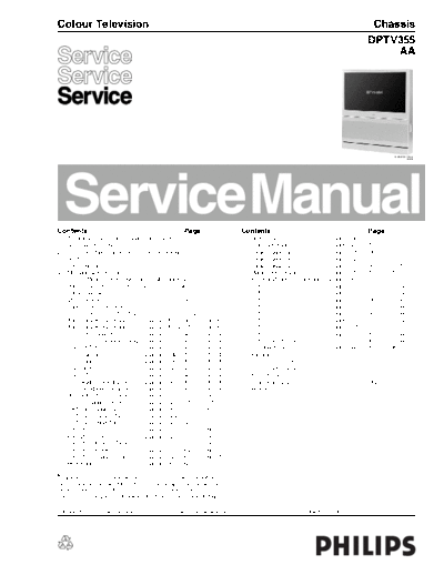
Image preview - the first page of the document
philips_dptv355_aa


>> Download philips_dptv355_aa documenatation <<

Text preview - extract from the document
Colour Television                                                                                                                     Chassis
                                                                                                                                     DPTV355
                                                                                                                                          AA


                                                                                                                                    55" model


                                                                                                                                                 CL 26532103_100.eps
                                                                                                                                                             050902


Contents                                                   Page                   Contents                                           Page
1   Technical Specifications, Connection Facilities,                                 HOP Panel                      (Diagram H2)     69         70-71
    and Chassis Overview                             2                               Side Jack Panel                (Diagram I/O)    72         73
2   Safety and Maintenance Instructions, Warnings,                                   Large Signal Panel             (Diagram L1)     74         77-78
    and Notes                                        5                               Large Signal Panel             (Diagram L2)     75         77-78
3   Directions for Use                               7                               Large Signal Panel             (Diagram L3)     76         77-78
4   Mechanical Instructions                          21                              Mains Switch Panel             (Diagram M1)     79         79
5   Service Modes, Error Codes, and Fault Finding 25                                 Keyboard/Light Sensor Panel    (Diagram P1)     80         81
6   Wiring Diagram, I2C, and Supply Lines Overview                                   SSM                            (Diagram S1)     82         91-94
    Wiring Diagram                                   33                              SSM                            (Diagram S2)     83         91-94
    I2C Overview                                     34                              SSM                            (Diagram S3)     84         91-94
    Supply Lines Overview                            35                              SSM                            (Diagram S4)     85         91-94
7   Circuit Diagrams and PWB Layouts                 Diagram         PWB             SSM                            (Diagram S5)     86         91-94
    Auto Convergence Panel         (Diagram ACS1) 36                 38-39           SSM                            (Diagram S6)     87         91-94
    Auto Convergence Panel         (Diagram ACS2) 37                 38-39           SSM                            (Diagram S7)     88         91-94
    SSB: SIM Connector             (Diagram B1)      40              49-54           SSM                            (Diagram S8)     89         91-94
    SSB: IF, I/O Videoprocessing (Diagram B2)        41              49-54           SSM: Diversity Tables                           90         91-94
    SSB: PICNIC                    (Diagram B3A) 42                  49-54           AC Input Panel                 (Diagram W)      95         96
    SSB: Falconic                  (Diagram B3B) 43                  49-54        8 Alignments                                       97
    SSB: Eagle                     (Diagram B3C) 44                  49-54        9 Circuit Descriptions                             103
    SSB: HOP                      (Diagram B4)       45              49-54           List of Abbreviations                           129
    SSB: OTC                      (Diagram B5)       46              49-54           IC Data Sheets                                  133
    SSB: Audio Demodulator        (Diagram B6)       47              49-54        10 Spare Parts List                                142
    SSB: Headphone Amplifier       (Diagram B10) 48                  49-54        11 Revision List                                   156
    3D Comb Filter (Optional)     (Diagram CB1) 55                   56
    Center Channel Switch         (Diagram CH1) 57                   57
    CRT Panel: Blue Tube           (Diagram D(B)1) 58                61
    CRT Panel: Green Tube         (Diagram D(G)1)59                  61
    CRT Panel: Red Tube            (Diagram D(R)1) 60                61
    PIP / DW                       (Diagram F1)      62              66-67
    PIP / DW: Tuner                (Diagram F2)      63              66-67
    PIP / DW: Diversity Table                        63              66-67
    PIP / DW: I/O Processing       (Diagram F3)      64              66-67
    PIP / DW: IF Video Sync        (Diagram F4)      65              66-67
    HOP Panel                      (Diagram H1) 68                   70-71


◦ Jabse Service Manual Search 2024 ◦ Jabse PravopisonTap.bg ◦ Other service manual resources online : FixyaeServiceinfo