Service Manuals, User Guides, Schematic Diagrams or docs for : Samsung Cam VP-D10 samsung_vp-d102d_vp-d10_ch7_sch
<< Back | HomeMost service manuals and schematics are PDF files, so You will need Adobre Acrobat Reader to view : Acrobat Download Some of the files are DjVu format. Readers and resources available here : DjVu Resources
For the compressed files, most common are zip and rar. Please, extract files with Your favorite compression software ( WinZip, WinRAR ... ) before viewing. If a document has multiple parts, You should download all, before extracting.
Good luck. Repair on Your own risk. Make sure You know what You are doing.
Image preview - the first page of the document
>> Download samsung_vp-d102d_vp-d10_ch7_sch documenatation <<
Text preview - extract from the document
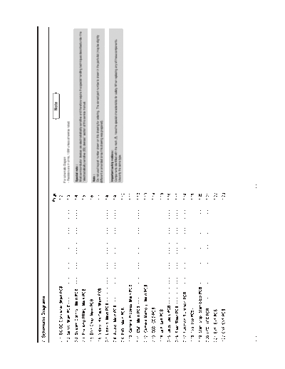
7. Schematic Diagrams

                                                                                                       Page                                                                            Note
7-1 DC/DC Converter (Main PCB) - - - - - - - - - - - - - - - - - - - - - - - - - - - - - - - - - 7-2
                                                                                                                       For schematic Diagram
7-2 Servo (Main PCB)- - - - - - - - - - - - - - - - - - - - - - - - - - - - - - - - - - - - - - - - - 7-3              - Resistors are in ohms, 1/8W unless otherwise noted.

7-3 System Control (Main PCB) - - - - - - - - - - - - - - - - - - - - - - - - - - - - - - - - - - 7-4                   Special note :
                                                                                                                        Most semiconductor devices are electrostatically sensitive and therefore require the special handling techniques described under the
7-4 Pre Amp/PRML (Main PCB) - - - - - - - - - - - - - - - - - - - - - - - - - - - - - - - - - - 7-5                     "electrostatically sensitive (ES) devices" section of this service manual.

7-5 DV1-Chip (Main PCB) - - - - - - - - - - - - - - - - - - - - - - - - - - - - - - - - - - - - - - 7-6                 Note :
                                                                                                                        Do not use the part number shown on this drawing for ordering. The correct part number is shown in the parts list (may be slightly
7-6 Video-Interface (Main PCB)- - - - - - - - - - - - - - - - - - - - - - - - - - - - - - - - - - 7-7                  different or amended since this drawing was prepared).

7-7 Line-In (Main PCB) - - - - - - - - - - - - - - - - - - - - - - - - - - - - - - - - - - - - - - - - 7-8
                                                                                                                        Important safety notices :
7-8 Audio (Main PCB) - - - - - - - - - - - - - - - - - - - - - - - - - - - - - - - - - - - - - - - - 7-9                Components identified with the mark      have the special characteristics for safety. When replacing any of these components.
                                                                                                                        Use only the same type.
7-9 PHY (Main PCB)- - - - - - - - - - - - - - - - - - - - - - - - - - - - - - - - - - - - - - - - - - 7-10
7-10 Camera Process (Main PCB) - - - - - - - - - - - - - - - - - - - - - - - - - - - - - - - - 7-11
7-11 DSP (Main PCB) - - - - - - - - - - - - - - - - - - - - - - - - - - - - - - - - - - - - - - - - - 7-12
7-12 Camera Memory (Main PCB) - - - - - - - - - - - - - - - - - - - - - - - - - - - - - - - - 7-13
7-13 CCD (CCD PCB)- - - - - - - - - - - - - - - - - - - - - - - - - - - - - - - - - - - - - - - - - - 7-14
7-14 Left (Left PCB) - - - - - - - - - - - - - - - - - - - - - - - - - - - - - - - - - - - - - - - - - - 7-15
7-15 Jack (Jack PCB)- - - - - - - - - - - - - - - - - - - - - - - - - - - - - - - - - - - - - - - - - 7-16
7-16 Rear (Rear PCB) - - - - - - - - - - - - - - - - - - - - - - - - - - - - - - - - - - - - - - - - - 7-17
7-17 Function (Function PCB) - - - - - - - - - - - - - - - - - - - - - - - - - - - - - - - - - - - 7-18
7-18 Top (Top PCB)- - - - - - - - - - - - - - - - - - - - - - - - - - - - - - - - - - - - - - - - - - - 7-19
7-19 Start-Stop (Start-Stop PCB) - - - - - - - - - - - - - - - - - - - - - - - - - - - - - - - - - 7-20
7-20 LCD (LCD PCB) - - - - - - - - - - - - - - - - - - - - - - - - - - - - - - - - - - - - - - - - - - 7-21
7-21 EVF (EVF PCB) - - - - - - - - - - - - - - - - - - - - - - - - - - - - - - - - - - - - - - - - - - 7-22
7-22 CVF (CVF PCB) - - - - - - - - - - - - - - - - - - - - - - - - - - - - - - - - - - - - - - - - - - 7-23


Samsung Electronics                                                                           This Document can not be used without Samsung's authorization                                                                                                    7-1
Schematic Diagrams


7-1 DC/DC Converter (Main PCB)


7-2                              This Document can not be used without Samsung's authorization   Samsung Electronics
                                                                                       Schematic Diagrams


7-2 Servo (Main PCB)


Samsung Electronics    This Document can not be used without Samsung's authorization                 7-3
Schematic Diagrams


7-3 System Control (Main PCB)


7-4                             This Document can not be used without Samsung's authorization   Samsung Electronics
                                                                                              Schematic Diagrams


7-4 Pre Amp/PRML (Main PCB)


Samsung Electronics           This Document can not be used without Samsung's authorization                 7-5
Schematic Diagrams


7-5 DV1-Chip (Main PCB)


7-6                       This Document can not be used without Samsung's authorization   Samsung Electronics
                                                                                                 Schematic Diagrams


7-6 Video-Interface (Main PCB)


Samsung Electronics              This Document can not be used without Samsung's authorization                 7-7
Schematic Diagrams


7-7 Line-In (Main PCB)


7-8                      This Document can not be used without Samsung's authorization   Samsung Electronics
                                                                                       Schematic Diagrams


7-8 Audio (Main PCB)


Samsung Electronics    This Document can not be used without Samsung's authorization                 7-9
Schematic Diagrams


7-9 PHY (Main PCB)


7-10                 This Document can not be used without Samsung's authorization   Samsung Electronics
                                                                                                 Schematic Diagrams


7-10 Camera Process (Main PCB)


Samsung Electronics              This Document can not be used without Samsung's authorization                7-11
Schematic Diagrams


7-11 DSP (Main PCB)


7-12                  This Document can not be used without Samsung's authorization   Samsung Electronics
                                                                                                Schematic Diagrams


7-12 Camera Memory (Main PCB)


Samsung Electronics             This Document can not be used without Samsung's authorization                7-13
Schematic Diagrams


7-13 CCD (CCD PCB)


7-14                 This Document can not be used without Samsung's authorization   Samsung Electronics
                                                                                       Schematic Diagrams


7-14 Left (Left PCB)


Samsung Electronics    This Document can not be used without Samsung's authorization                7-15
Schematic Diagrams


7-15 Jack (Jack PCB)


7-16                   This Document can not be used without Samsung's authorization   Samsung Electronics
                                                                                       Schematic Diagrams


7-16 Rear (Rear PCB)


Samsung Electronics    This Document can not be used without Samsung's authorization                7-17
Schematic Diagrams


7-17 Function (Function PCB)


7-18                           This Document can not be used without Samsung's authorization   Samsung Electronics
                                                                                      Schematic Diagrams


7-18 Top (Top PCB)


Samsung Electronics   This Document can not be used without Samsung's authorization                7-19
Schematic Diagrams


7-19 Start-Stop (Start-Stop PCB)


7-20                               This Document can not be used without Samsung's authorization   Samsung Electronics
                                                                                      Schematic Diagrams


7-20 LCD (LCD PCB)


Samsung Electronics   This Document can not be used without Samsung's authorization                7-21
Schematic Diagrams


7-21 EVF (EVF PCB)


7-22                 This Document can not be used without Samsung's authorization   Samsung Electronics
                                                                                      Schematic Diagrams


7-22 CVF (CVF PCB)


Samsung Electronics   This Document can not be used without Samsung's authorization                7-23
Schematic Diagrams


                                             MEMO


7-24                 This Document can not be used without Samsung's authorization   Samsung Electronics
◦ Jabse Service Manual Search 2024 ◦ Jabse Pravopis ◦ onTap.bg ◦ Other service manual resources online : Fixya ◦ eServiceinfo