Service Manuals, User Guides, Schematic Diagrams or docs for : Samsung Cam VP-D351 15_Schematic Diagram
<< Back | HomeMost service manuals and schematics are PDF files, so You will need Adobre Acrobat Reader to view : Acrobat Download Some of the files are DjVu format. Readers and resources available here : DjVu Resources
For the compressed files, most common are zip and rar. Please, extract files with Your favorite compression software ( WinZip, WinRAR ... ) before viewing. If a document has multiple parts, You should download all, before extracting.
Good luck. Repair on Your own risk. Make sure You know what You are doing.
Image preview - the first page of the document
>> Download 15_Schematic Diagram documenatation <<
Text preview - extract from the document
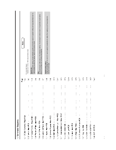
10. Schematic Diagrams

                                                                                                      Page                                                                            Note
10-1 DC/DC Converter (Main PCB) - - - - - - - - - - - - - - - - - - - - - - - - - - - - - - - - 10-2
                                                                                                                      For schematic Diagram
                                                                                                                      - Resistors are in ohms, 1/8W unless otherwise noted.
10-2 Servo (Main PCB) - - - - - - - - - - - - - - - - - - - - - - - - - - - - - - - - - - - - - - - - 10-3
                                                                                                                       Special note :
10-3 System Control (Main PCB) - - - - - - - - - - - - - - - - - - - - - - - - - - - - - - - - - 10-4                  Most semiconductor devices are electrostatically sensitive and therefore require the special handling techniques described under the
                                                                                                                       "electrostatically sensitive (ES) devices" section of this service manual.
10-4 Pre Amp/PRML (Main PCB) - - - - - - - - - - - - - - - - - - - - - - - - - - - - - - - - - 10-5
                                                                                                                       Note :
10-5 DV-1Chip (Main PCB) - - - - - - - - - - - - - - - - - - - - - - - - - - - - - - - - - - - - - 10-6                Do not use the part number shown on this drawing for ordering. The correct part number is shown in the parts list (may be slightly
                                                                                                                      different or amended since this drawing was prepared).
10-6 Video-Interface (Main PCB) - - - - - - - - - - - - - - - - - - - - - - - - - - - - - - - - - 10-7
                                                                                                                       Important safety notices :
10-7 Audio (Main PCB) - - - - - - - - - - - - - - - - - - - - - - - - - - - - - - - - - - - - - - - - 10-8             Components identified with the mark      have the special characteristics for safety. When replacing any of these components.
                                                                                                                       Use only the same type.
10-8 Camera Process (Main PCB) - - - - - - - - - - - - - - - - - - - - - - - - - - - - - - - - 10-9

10-9 DSP (Main PCB) - - - - - - - - - - - - - - - - - - - - - - - - - - - - - - - - - - - - - - - - - 10-10

10-10 Camera Memory 1 (Main PCB) - - - - - - - - - - - - - - - - - - - - - - - - - - - - - - 10-11

10-11 Camera Memory 2 (Main PCB) - - - - - - - - - - - - - - - - - - - - - - - - - - - - - - 10-12

10-12 CCD (CCD PCB) - - - - - - - - - - - - - - - - - - - - - - - - - - - - - - - - - - - - - - - - - 10-13

10-13 Left (Left PCB)- - - - - - - - - - - - - - - - - - - - - - - - - - - - - - - - - - - - - - - - - - 10-14

10-14 Jack (Jack PCB) - - - - - - - - - - - - - - - - - - - - - - - - - - - - - - - - - - - - - - - - 10-15

10-15 Rear (Rear PCB) - - - - - - - - - - - - - - - - - - - - - - - - - - - - - - - - - - - - - - - - 10-16

10-16 Function (Function PCB)- - - - - - - - - - - - - - - - - - - - - - - - - - - - - - - - - - - 10-17

10-17 Top (Top PCB) - - - - - - - - - - - - - - - - - - - - - - - - - - - - - - - - - - - - - - - - - - 10-18

10-18 CVF (CVF PCB) - - - - - - - - - - - - - - - - - - - - - - - - - - - - - - - - - - - - - - - - - 10-19

10-19 LCD (LCD PCB) - - - - - - - - - - - - - - - - - - - - - - - - - - - - - - - - - - - - - - - - - 10-20

10-20 EVF (EVF PCB)- - - - - - - - - - - - - - - - - - - - - - - - - - - - - - - - - - - - - - - - - - 10-21


Samsung Electronics                                                                          This Document can not be used without Samsung's authorization                                                                                                  10-1
Schematic Diagrams


10-1 DC/DC Converter (Main PCB)


10-2                              This Document can not be used without Samsung's authorization   Samsung Electronics
                                                                                        Schematic Diagrams


10-2 Servo (Main PCB)


Samsung Electronics     This Document can not be used without Samsung's authorization                10-3
Schematic Diagrams


10-3 System Control (Main PCB)


10-4                             This Document can not be used without Samsung's authorization   Samsung Electronics
                                                                                               Schematic Diagrams


10-4 Pre Amp/PRML (Main PCB)


Samsung Electronics            This Document can not be used without Samsung's authorization                10-5
Schematic Diagrams


10-5 DV-1Chip (Main PCB)


10-6                       This Document can not be used without Samsung's authorization   Samsung Electronics
                                                                                                  Schematic Diagrams


10-6 Video-Interface (Main PCB)


Samsung Electronics               This Document can not be used without Samsung's authorization                10-7
Schematic Diagrams


10-7 Audio (Main PCB)


10-8                    This Document can not be used without Samsung's authorization   Samsung Electronics
                                                                                                 Schematic Diagrams


10-8 Camera Process (Main PCB)


Samsung Electronics              This Document can not be used without Samsung's authorization                10-9
Schematic Diagrams


10-9 DSP (Main PCB)


10-10                 This Document can not be used without Samsung's authorization   Samsung Electronics
                                                                                                   Schematic Diagrams


10-10 Camera Memory 1 (Main PCB)


Samsung Electronics                This Document can not be used without Samsung's authorization               10-11
Schematic Diagrams


10-11 Camera Memory 2 (Main PCB)


10-12                              This Document can not be used without Samsung's authorization   Samsung Electronics
                                                                                      Schematic Diagrams


10-12 CCD (CCD PCB)


Samsung Electronics   This Document can not be used without Samsung's authorization               10-13
Schematic Diagrams


10-13 Left (Left PCB)


10-14                   This Document can not be used without Samsung's authorization   Samsung Electronics
                                                                                        Schematic Diagrams


10-14 Jack (Jack PCB)


Samsung Electronics     This Document can not be used without Samsung's authorization               10-15
Schematic Diagrams


10-15 Rear (Rear PCB)


10-16                   This Document can not be used without Samsung's authorization   Samsung Electronics
                                                                                                Schematic Diagrams


10-16 Function (Function PCB)


Samsung Electronics             This Document can not be used without Samsung's authorization               10-17
Schematic Diagrams


10-17 Top (Top PCB)


10-18                 This Document can not be used without Samsung's authorization   Samsung Electronics
                                                                                      Schematic Diagrams


10-18 CVF (CVF PCB)


Samsung Electronics   This Document can not be used without Samsung's authorization               10-19
Schematic Diagrams


10-19 LCD (LCD PCB)


10-20                 This Document can not be used without Samsung's authorization   Samsung Electronics
                                                                                      Schematic Diagrams


10-20 EVF (EVF PCB)


Samsung Electronics   This Document can not be used without Samsung's authorization               10-21
Schematic Diagrams


                                             MEMO


10-22                This Document can not be used without Samsung's authorization   Samsung Electronics
◦ Jabse Service Manual Search 2024 ◦ Jabse Pravopis ◦ onTap.bg ◦ Other service manual resources online : Fixya ◦ eServiceinfo