Service Manuals, User Guides, Schematic Diagrams or docs for : Samsung Audio HT-DL200 SAMSUNG_HT-DL200
<< Back | HomeMost service manuals and schematics are PDF files, so You will need Adobre Acrobat Reader to view : Acrobat Download Some of the files are DjVu format. Readers and resources available here : DjVu Resources
For the compressed files, most common are zip and rar. Please, extract files with Your favorite compression software ( WinZip, WinRAR ... ) before viewing. If a document has multiple parts, You should download all, before extracting.
Good luck. Repair on Your own risk. Make sure You know what You are doing.
Image preview - the first page of the document
>> Download SAMSUNG_HT-DL200 documenatation <<
Text preview - extract from the document
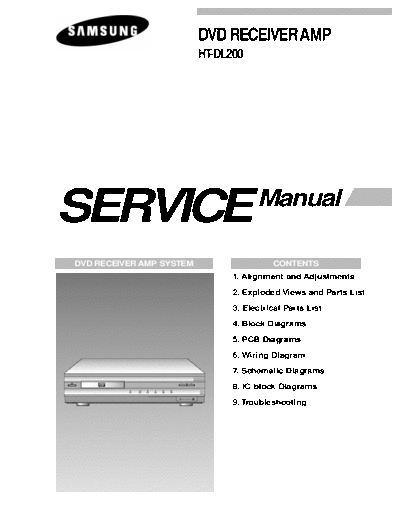
                                         DVD RECEIVER AMP
                                         HT-DL200


SERVICE                                              Manual

DVD RECEIVER AMP SYSTEM                                   CONTENTS
                                               1. Alignment and Adjustments

                                               2. Exploded Views and Parts List

                                               3. Electrical Parts List

                                               4. Block Diagrams

                                               5. PCB Diagrams

                                               6. Wiring Diagram

                                               7. Schematic Diagrams
                                Volume


    VIDEO


            Function
                                               8. IC block Diagrams
                       Phones


                                               9. Troubleshooting
8. IC Block Digrams
8-1 Main
1. 74CX244

           LOW VOLTAGE CMOS OCTAL BUS BUFFER (3-STATE)
                  WITH 5V TOLERANT INPUTS AND OUTPUTS
       s   5V TOLERANT INPUTS AND OUTPUTS
       s   HIGH SPEED:
           tPD = 6.5 ns (MAX.) at VCC = 3V
       s   POWER-DOWN PROTECTION ON INPUTS
           AND OUTPUTS
       s   SYMMETRICAL OUTPUT IMPEDANCE:                               M                       T
           |IOH| = IOL = 24 mA (MIN)                            (Micro Package)          (TSSOP Package)
       s   PCI BUS LEVELS GUARANTEED AT 24mA                             ORDER CODES :
       s   BALANCED PROPAGATION DELAYS:                            74LCX244M      74LCX244T
           tPLH  tPHL
       s   OPERATING VOLTAGE RANGE:
           VCC (OPR) = 2.0V to 3.6V (1.5V Data Retention)
                                                            inputs and outputs.
       s   PIN AND FUNCTION COMPATIBLE WITH
           74 SERIES 244                                    It has same speed performance at 3.3V than 5V
       s   LATCH-UP PERFORMANCE EXCEEDS 500mA               AC/ACT family, combined with a lower power
       s   ESD PERFORMANCE:                                 consumption.
            HBM >2000V; MM > 200V                           This device is designed to be used with 3 state
                                                            memory address drivers, etc.
       DESCRIPTION                                          All inputs and outputs are equipped with
       The LCX244 is a low voltage CMOS OCTAL BUS           protection circuits against static discharge, giving
       BUFFER (NON-INVERTED) fabricated with                them 2KV ESD immunity and transient excess
       sub-micron silicon gate and double-layer metal       voltage.
       wiring C2MOS technology. It is ideal for low
       power and high speed 3.3V applications; it can
       be interfaced to 5V signal environment for both

       PIN CONNECTION AND IEC LOGIC SYMBOLS


Samsung Electronics                                                                                                8-1
2. 74VHC244

      74VHC244
      Octal Buffer/Line Driver with 3-STATE Outputs
      General Description                                                             cuit prevents device destruction due to mismatched supply
                                                                                      and input voltages.
      The VHC244 is an advanced high speed CMOS octal bus
      buffer fabricated with silicon gate CMOS technology. It
      achieves high speed operation similar to equivalent Bipolar
                                                                                      Features
      Schottky TTL while maintaining the CMOS low power dissi-                        s High Speed: tPD = 3.9ns (typ) at VCC = 5V
      pation. The VHC244 is a non-inverting 3-STATE buffer hav-                       s High noise immunity: VNIH = VNIL = 28% VCC (min)
      ing two active-LOW output enables. These devices are
      designed to be used as 3-STATE memory address drivers,                          s Power down protection is provided on all inputs
      clock drivers, and bus oriented transmitter/receivers.                          s Low noise: VOLP = 0.6V (typ)
      An input protection circuit ensures that 0V to 7V can be                        s Low power dissipation: ICC = 4
◦ Jabse Service Manual Search 2024 ◦ Jabse Pravopis ◦ onTap.bg ◦ Other service manual resources online : Fixya ◦ eServiceinfo