Service Manuals, User Guides, Schematic Diagrams or docs for : Samsung Audio MX-HS9000 samsung_mx_hs9000
<< Back | HomeMost service manuals and schematics are PDF files, so You will need Adobre Acrobat Reader to view : Acrobat Download Some of the files are DjVu format. Readers and resources available here : DjVu Resources
For the compressed files, most common are zip and rar. Please, extract files with Your favorite compression software ( WinZip, WinRAR ... ) before viewing. If a document has multiple parts, You should download all, before extracting.
Good luck. Repair on Your own risk. Make sure You know what You are doing.
Image preview - the first page of the document
>> Download samsung_mx_hs9000 documenatation <<
Text preview - extract from the document
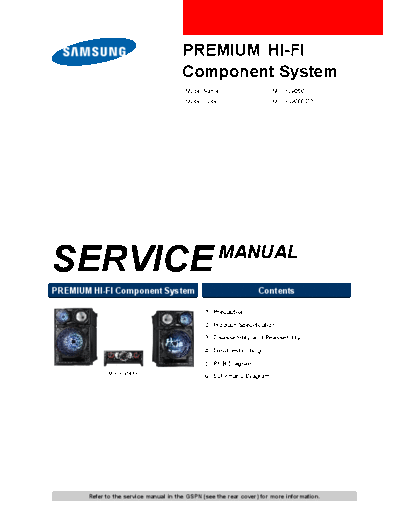
                                        PREMIUM HI-FI
                                        Component System
                                         Model Name                     MX-HS9000
                                         Model Code                     MX-HS9000/ZP


SERVICE                                               MANUAL
PREMIUM HI-FI Component System                                     Contents

                                                1. Precaution

                                                2. Product Specification

                                                3. Disassembly and Reassembly

                                                4. Troubleshooting

                                                5. PCB Diagram
             MX-HS9000                          6. Schematic Diagram


       Refer to the service manual in the GSPN (see the rear cover) for more information.
Contents


Contents
1.   Precaution........................................................................................................................................ 1 - 1
     1.1.     Safety Precautions ................................................................................................................... 1 - 1
     1.2.     Servicing Precautions ............................................................................................................... 1 - 3
     1.3.     Precautions for Electrostatically Sensitive Devices (ESDs) .............................................................. 1 - 4
     1.4.     Installation Precautions ............................................................................................................. 1 - 5
2.   Product Specification ......................................................................................................................... 2 - 1
     2.1.     Product Feature ....................................................................................................................... 2 - 1
     2.2.     Specifications.......................................................................................................................... 2 - 2
     2.3.     Specifications Analysis ............................................................................................................. 2 - 3
     2.4.     Accessories ............................................................................................................................ 2 - 4
              2.4.1.     Supplied Accessories ................................................................................................... 2 - 4
3.   Disassembly and Reassembly .............................................................................................................. 3 - 1
     3.1.     Overall Disassembly and Reassembly .......................................................................................... 3 - 1
     3.2.     DECK Disassembly and Reassembly ........................................................................................... 3 - 12
4.   Troubleshooting ................................................................................................................................ 4 - 1
     4.1.     Checkpoints by Error Mode ....................................................................................................... 4 - 1
              4.1.1.     No Power................................................................................................................... 4 - 2
              4.1.2.     No Output .................................................................................................................. 4 - 4
     4.2.     Measures to be taken when the Protection Circuit operates............................................................... 4 - 6
              4.2.1.     Operation of Power Block Protection Circuit .................................................................... 4 - 6
              4.2.2.     Check AMP in Power Protection .................................................................................... 4 - 7
     4.3.     MICOM, MPEG Initialization & Update ...................................................................................... 4 - 8
     4.4.     Buyer-Region Code Setting Method ............................................................................................ 4 - 9
              4.4.1.     The inserting method of Region Code after replacing the Main PBA ..................................... 4 - 9
5.   PCB Diagram ................................................................................................................................... 5 - 1
     5.1.     Wiring Diagram....................................................................................................................... 5 - 1
     5.2.     FUNCTION PCB Top .............................................................................................................. 5 - 2
              5.2.1.     Pin Connection ........................................................................................................... 5 - 3
     5.3.     FUNCTION PCB Bottom.......................................................................................................... 5 - 4
     5.4.     VFD PCB Top/Bottom.............................................................................................................. 5 - 5
              5.4.1.     Pin Connection ........................................................................................................... 5 - 6
     5.5.     LED PCB Bottom .................................................................................................................... 5 - 7
              5.5.1.     Pin Connection ........................................................................................................... 5 - 8
     5.6.     MAIN PCB Top ...................................................................................................................... 5 - 9
              5.6.1.     Pin Connection ........................................................................................................... 5 - 10
              5.6.2.     Test Point Wave Form .................................................................................................. 5 - 11
     5.7.     MAIN PCB Bottom.................................................................................................................. 5 - 12
     5.8.     SMPS PCB Top....................................................................................................................... 5 - 13

i                                                                                     Copyright
◦ Jabse Service Manual Search 2024 ◦ Jabse Pravopis ◦ onTap.bg ◦ Other service manual resources online : Fixya ◦ eServiceinfo