Service Manuals, User Guides, Schematic Diagrams or docs for : Samsung DVD DTB-P850V block_diagram_221

<< Back | Home

Most service manuals and schematics are PDF files, so You will need Adobre Acrobat Reader to view : Acrobat Download Some of the files are DjVu format. Readers and resources available here : DjVu Resources
For the compressed files, most common are zip and rar. Please, extract files with Your favorite compression software ( WinZip, WinRAR ... ) before viewing. If a document has multiple parts, You should download all, before extracting.
Good luck. Repair on Your own risk. Make sure You know what You are doing.


Image preview - the first page of the document
block_diagram_221


>> Download block_diagram_221 documenatation <<

Text preview - extract from the document
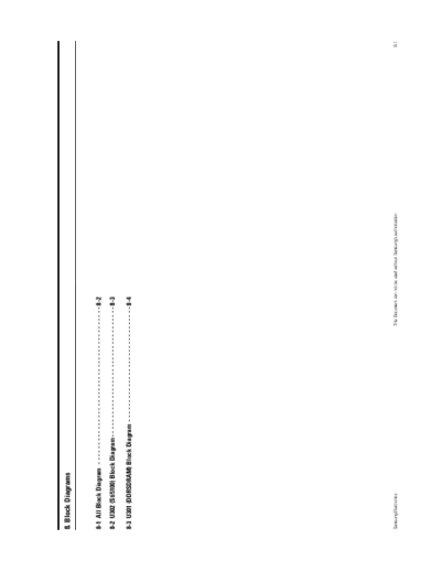
8. Block Diagrams


8-1 All Block Diagram - - - - - - - - - - - - - - - - - - - - - - - - - - - - - - - - - - - - - - - - - 8-2

8-2 U302 (Sti5100) Block Diagram - - - - - - - - - - - - - - - - - - - - - - - - - - - - - - - - - - 8-3

8-3 U301 (DDRSDRAM) Block Diagram - - - - - - - - - - - - - - - - - - - - - - - - - - - - - - 8-4


Samsung Electronics                                                                          This Document can not be used without Samsung's authorization   8-1
Block Diagrams


8-1 All Block Diagram


                 J1201                                       J703

                                                                                                                                                              U504
                                 J702
                                                                                                          J801
                                               J701                                                                                                  MOD101
                         U1201
                                                                                                 U701
                                                                                                                            TM102            TM201


                                                                                                                                                              CN1001


                 HU1


                                        X702
                                                                                                                                    U602~5


                                                                      U302


                                                                                                                                                              CN601
                                                      U301
                                                                                                   U401


                                                                                              J1202


8-2                                                                 This Document can not be used without Samsung's authorization                             Samsung Electronics
                                                                                                                                                                                         Block Diagrams


8-2 U302 (Sti5100) Block Diagram


                                Shared         DDR SDRAM                                                                                         ROM/             SDRAM
                                Memory       128/256/512 Mbit                                               RGB/YUV                 YC or        SFlash          peeripheral
                                                                                                              out                   CVBS
                 ST20 C2+ Core
                                                                                                                          PAL                                                   Memory/bus
                          8K ICache                                                                 Blitter                                                FMI
               DCJ                                                          Video                    and                 NTSC                                                  Request/grant
                                                  LMI           USB
                            Int.Control                                    Decoder                   tile               SECAM
           4K SRAM                                              2.0                                 RAM
                                                                                                                                             Te;etext
                           8K DCache                                                                                    TV out              omterface


                                                                                                                                                                                S/PDIF
                                                    2x I/F         IR            MAFE I/F                                            4X                      Audio
                           Transport Steam                                                                  PWM                                                                  out
           PTI                                     SmCard        Tx/Rx          amd SiLabs                                           PIO        Central     decoder
                               merger
                                                                                      4x                       3x                                DMA
                                                   DisEqC         ILC                                                                DC0                     Audio
                                                                                     UARTs                    SSCs
                                                                                                                                                             DACs
                       TS0IN     TS2IN  TS1IN                                                                                                             Analog audio
                      ser/par   TS2OUT par/D1                                                                                                               out L/R
                                1394OUT


Samsung Electronics                                                      This Document can not be used without Samsung's authorization                                                             8-3
Block Diagrams


8-3 U301 (DDRSDRAM) Block Diagram


                 CKE        Control Logic
                 CK
                 CK
                 CS                  command
                 WE                   Decode
                 CAS                                                                                                                                   Bank3
                 RAS                                                                                                          Bank1 Bank2                                                                              CK, CK
                                                Mode
                                                              Row-address MUX
                                               Registers


                                                                                        Row-Address latch
                                                                                                                                                                                                                        DLL


                                                                                           &Decoder
                                           15         13                        13                                             Bank0


                                                                                             Bank0
                                                                                                                 8192         Memory


                                                                                                                                                                          Read Latch
                                                                                                                               Array
                                                                                                                                                                                       16                    Data


                                                                                                                                                                                                                         Drivers
                                                                                                                           (8192x512x32)                                                    Mux
                                                                                                                                                                 32                                    16
                                                                                                                                                                                       16
                                                                                                                         Sense Amplifier
                                                                                                                                                                                                        DOS
                                                                                                                                                                                                                   1
                                                                           13
                                                                                                                                                                                                      Generator
                                                             Refresh Counter


                                                                                                                          16384                                                             COL0
                                                                                        Bank Control Logic
                            Address Register


                                                                                                                                                              32                                                   DQS
                                                                                                                           I/O GATING                                                               Input
                       15                                                           2                                                                                                                                               DQ0-
                                                                                                                          DM Mask Logic                                                            Regiser
                                                                                                                                                                                            Mask 1       1                          DQ15,
                                                                                                                                                                      Write                                 2                       LDM,
                                                                                                                                                                                                 1


                                                                                                                                                                                                                        Receivers
                                                                                                                                                                                            2             1                         UDM
                                                                                2                                                          512(x32)                32 FIFO
                                                                                                                                                                                                 16         16
                                                                                                             9                 Column                                    &                  Data                  16
                  A0-A12,                           10 Column-address                                                                                                 Drivers                    16         16
                 BA0, BA1                                                                                    1                 Decoder                                                      32
                                                        Conuter/Latch                                            COL0                                                                                                               LDQS,
                                                                                                                                                                        CK,CK                      COL0            2                UDQS


8-4                                                                                                                 This Document can not be used without Samsung's authorization                                                       Samsung Electronics


◦ Jabse Service Manual Search 2024 ◦ Jabse PravopisonTap.bg ◦ Other service manual resources online : FixyaeServiceinfo