Service Manuals, User Guides, Schematic Diagrams or docs for : Samsung DVD DTB-P850V contents_178
<< Back | HomeMost service manuals and schematics are PDF files, so You will need Adobre Acrobat Reader to view : Acrobat Download Some of the files are DjVu format. Readers and resources available here : DjVu Resources
For the compressed files, most common are zip and rar. Please, extract files with Your favorite compression software ( WinZip, WinRAR ... ) before viewing. If a document has multiple parts, You should download all, before extracting.
Good luck. Repair on Your own risk. Make sure You know what You are doing.
Image preview - the first page of the document

>> Download contents_178 documenatation <<
Text preview - extract from the document
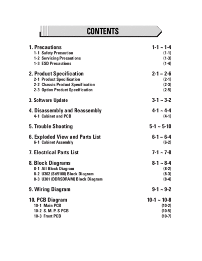
                              CONTENTS
1. Precautions                             1-1 ~ 1-4
  1-1 Safety Precaution                         (1-1)
  1-2 Servicing Precautions                     (1-3)
  1-3 ESD Precautions                           (1-4)

2. Product Specification                   2-1 ~ 2-6
  2-1 Product Specification                     (2-1)
  2-2 Chassis Product Specification             (2-3)
  2-3 Option Product Specification              (2-5)

3. Software Update                         3-1 ~ 3-2
4. Disassembly and Reassembly              4-1 ~ 4-4
  4-1 Cabinet and PCB                           (4-1)

5. Trouble Shooting                       5-1 ~ 5-10
6. Exploded View and Parts List            6-1 ~ 6-4
  6-1 Cabinet Assembly                          (6-2)

7. Electrical Parts List                   7-1 ~ 7-8
8. Block Diagrams                          8-1 ~ 8-4
  8-1 All Block Diagram                         (8-2)
  8-2 U302 (Sti5100) Block Diagram              (8-3)
  8-3 U301 (DDRSDRAM) Block Diagram             (8-4)

9. Wiring Diagram                          9-1 ~ 9-2
10. PCB Diagram                          10-1 ~ 10-8
  10-1 Main PCB                                (10-2)
  10-2 S. M. P. S PCB                          (10-5)
  10-3 Front PCB                               (10-7)
                                CONTENTS
11. Schematic Diagrams                         11-1 ~ 11-16
  11-1 S. M. P. S (S. M. P. S PCB)                    (11-2)
  11-2 Tuner, Demodulator1(Main PCB)                  (11-3)
  11-3 Tuner, Demodulator2 (Main PCB)                 (11-4)
  11-4 DDR Interface (Main PCB)                       (11-5)
  11-5 Flash Interface, PIO (Main PCB)                (11-6)
  11-6 TS Interface, USB2.0, JATG (Main PCB)          (11-7)
  11-7 ATA Interface (Main PCB)                       (11-8)
  11-8 A/V S/W Switch (Main PCB)                      (11-9)
  11-9 AV Output(SCART) (Main PCB)                   (11-10)
  11-10 STI5100 VCC& GND (Main PCB)                  (11-11)
  11-11 S-CARD,POWER (Main PCB)                      (11-12)
  11-12 MODEM (Main PCB)                             (11-13)
  11-13 RESET, RS232, EEPROM (Main PCB)              (11-14)
  11-14 Front (Front PCB)                            (11-15)

12. Operating Instructions                     12-1 ~ 12-24
13. Circuit Operating Description              13-1 ~ 13-16
  13-1   Splitter (MOD101)                            (13-1)
  13-2   Tuner (TM101, TM102)                         (13-1)
  13-3   Main Processor (U302)                        (13-2)
  13-4   Memory Interface                             (13-8)
  13-5   Video Out                                   (13-12)
  13-6   Audio Out                                   (13-13)
  13-7   Smart Card Interface (TDA8024)              (13-14)
  13-8   USB interface                               (13-15)

14. Reference Information                       14-1 ~ 14-2
  14-1 Terminology                                    (14-1)
◦ Jabse Service Manual Search 2024 ◦ Jabse Pravopis ◦ onTap.bg ◦ Other service manual resources online : Fixya ◦ eServiceinfo