Service Manuals, User Guides, Schematic Diagrams or docs for : Samsung DVD DVD-V6800 samsung_dvd-v6800_sch

<< Back | Home

Most service manuals and schematics are PDF files, so You will need Adobre Acrobat Reader to view : Acrobat Download Some of the files are DjVu format. Readers and resources available here : DjVu Resources
For the compressed files, most common are zip and rar. Please, extract files with Your favorite compression software ( WinZip, WinRAR ... ) before viewing. If a document has multiple parts, You should download all, before extracting.
Good luck. Repair on Your own risk. Make sure You know what You are doing.


Image preview - the first page of the document
samsung_dvd-v6800_sch


>> Download samsung_dvd-v6800_sch documenatation <<

Text preview - extract from the document
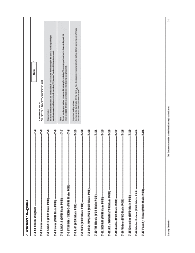
7. Schematic Diagrams

7-1 All block Diagram ----------------------------------------------------------------------------------------7-2                                                                              Note

                                                                                                                                     For schematic Diagram
7-2 Power ------------------------------------------------------------------------------------------------------------7-3           - Resistors are in ohms, /8W unless otherwise noted.


7-3 S.M.P.S (VCR Main PCB) ------------------------------------------------------------------------------7-5                        Special note :
                                                                                                                                    Most semiconductor devices are electrostatically sensitive and therefore require the special handling techniques
                                                                                                                                    described under the "electrostatically sensitive (ES) devices" section of this service manual.
7-4 Power (VCR Main PCB) --------------------------------------------------------------------------------7-6
                                                                                                                                    Note :
7-5 S.M.P.S (DVD Main PCB) ------------------------------------------------------------------------------7-7                        Do not use the part number shown on this drawing for ordering. The correct part number is shown in the parts list
                                                                                                                                    (may be slightly different or amended since this drawing was prepared).
7-6 SYSCON / SERVO (VCR Main PCB) --------------------------------------------------------------7-8
                                                                                                                                    Important safety notices :
7-7 A/V (VCR Main PCB) ----------------------------------------------------------------------------------7-10                       Components identified with the mark        have the special characteristics for safety. When replacing any of these
                                                                                                                                    components. Use only the same type.
7-8 Hi-Fi (VCR Main PCB) ---------------------------------------------------------------------------------7-12

7-9 OSD, VPS/PDC (VCR Main PCB) ----------------------------------------------------------------7-13

7-10 TM Block (VCR Main PCB) ------------------------------------------------------------------------7-14

7-11 SECAM (VCR Main PCB) ---------------------------------------------------------------------------7-15

7-12 A2 / NICAM (VCR Main PCB) -------------------------------------------------------------------7-16

7-13 Audio (DVD Main PCB) -----------------------------------------------------------------------------7-17

7-14 Video (DVD Main PCB) -----------------------------------------------------------------------------7-18

7-15 Decoder (DVD Main PCB) ------------------------------------------------------------------------7-19

7-16 Motor Driver (DVD Main PCB) -----------------------------------------------------------------7-20

7-17 Front / Timer (VCR Main PCB) -----------------------------------------------------------------7-21


Samsung Electronics                                                                      This Document can not be used without Samsung's authorization                                                                                                    7-
Schematic Diagrams


7-1 All block Diagram

                                                                                                                                               A/V Common

                        DECK ASS'Y


                                                                                   AUDIO R


                                                                                                                                                         AUDIO R
                                                                         AUDIO L


                                                                                                                                               AUDIO L
                                                            Coaxial


                                                                                                                                       VIDEO
                                                                                                              (RGB,CVBS)
                                                                                             Y   Pb   Pr      SCART JACK


                                                                                                               G     B      R
                                                                                                                                 CVBS


                                    Pick-up & I/V Amp


                                                                                                                                CVBS          IC802
           Disk Motor           Sled Motor                                                                                                 (BU4053)                         AUDIO L/R          IC501
                                                                                                                                       Output Signal Switch                                  (LA72646)
                                                                                                                                                                                        Hi-FI Audio Processor

                       MDIC1
                                                                                                                                 AUDIO L/R
                      (AM5766)
                     Motor Driver
                                                                                                                                                                                           IC301
                                                                                                                                                                                        (LA71750EM)
                                                                                                                                                                                    Video Signal Processor
                                                                        ZIC1                      DIC5 64MB SD RAM
                                                                       ZORAN
                                                                      ZR36966


                                                                                                               DIC7                          IC601
                                                                                                           (TC74VHCT125)                  (UPD78F4928)                                       IC605 EEPROM
                                                                                                            Level Shifter                VCR Main Micom


                                                                                                                                                 IC701
                                                             ZIC3
                                                                                                                                                (PT6961)
                                                         (MX25L1605A)
                                                                                                                                                LED Drive
                                                        IMB Flash Memory

                                                                                                                                                                                                            Front A/V Jack


                                                                                                                                                                   STEREO


                                                                                                                                                   (DT701)


7-                                                          This Document can not be used without Samsung's authorization                                                                                       Samsung Electronics
                                                                                                                                                                                                         Schematic Diagrams


7-2 Power

7-2-1 About S.M.P.S (Ringing Choke Converter Method)
                                                                                                                                                                         wSNUBBERCircuit:
                                                                                                                                                                          PDS11,PCD12,PRS13,PCD11,PPS12
q Terms
 1)1st:Commonpowerinputto1stwinding.
                                                                                                                                                                         1)Preventresidualhighvoltageattheterminalsof
 2)2nd:Circuitfollowingsoutputwindingoftransformer.
                                                                                                                                                                          switchduringswitchoff/Suppressnoise.
 3)f(Frequency):Switchingfrequency(T:Switchingcycle)
                                                                                                                                                                          Highinvertedpoweroccursatswitch(PQR11)off,
 4)Duty:(Ton/T)x100
                                                                                                                                                                          becauseofthe1stwindingoftransformer:
                                                                                                                                                                          (V=-L1xdi/dt.L1:LeakageInduction)
7-2-2 Circuit description [FLY-Back RCC(Ringing Choke Converter)] Control                                                                                                 Averyhighresidualvoltageexistonbothterminals
                                                                                                                                                                          ofPICF14,5~8pinbecausedtisaveryshort.
q AC Power Rectification/Smoothing Terminal
 1) PDS01, PDS02, PDS03, PDS04 : Convert AC power to DC(Full wave rectification).                                                                                        2)SNUBBERcircuitprotectsPQR11fromdamage
 2)PEF10:SmooththevoltageconvertedtoDC.                                                                                                                                   throughleakagevoltagesuppressionbyRC,
 3)PCD01,PCD02,PBS01:Noiseremovalatpowerinput/output.                                                                                                                     (ChargestheleakagevoltagetoPDS11,PER13,
 4)PVA1:SMPSprotectionatpowersurgeinput.                                                                                                                                  PCD12anddischargestoPRS11,PRS12).


                                                                                                                                                                    Fig. 7-2

                                                                                                                    eDrivingcircuit
                                                                                                                     WhenVinsupplied,drivingcurrentIgoccursthrouhgthePICF1.BythisI1(=HfexIg)
                                                                                                                     occursthrougthePICF1andtheVbisinductedtobasewindingcoilNB.
                                                                                                                     By inducted Vb, Ib start flow and the VCC voltage of PQR11 is sustained stable.
                                                                                                                     IbisconstantandI1increasesinProportiontotime.AfterconstanttimepassedIb
                                                                                                                     becometoshortageandPICF1iscutOFF(S/WOFF).


                                                    Fig. 7-1


Samsung Electronics                                                            This Document can not be used without Samsung's authorization                                                                         7-
Schematic Diagrams
                                                                                          q   Operationdescriptions
                                                                                              1)InternalOP-Amp`+'basepotentialofPICS2is2.5Vandexternal"-"inputpotentialis
                                                                                               connectedwithPRS33andPRS34tomaintainVoutof4.4V.
                                                                                              2)Ifloadof4.4Vterminalincrease(orACinoutvoltagedecrease)andVoutdecreaseover4.4V,
                                                                                               Then:PICS2"R"potentialdecreaseover2.5V-->PICS2A-KBASECurrentdecrease-->
                                                                                               PICS2A-KCurrentdecrease-->PICS1DIODECurrentdecrease-->PICS1C-ECurrentdecrease-->
                                                                                               PICS1C-EVoltageincrease-
                                                                                               ->PICS1F-BVoltageincrease-->OUTDUTYincreaseTRANSPrimaryCuttentIncrease-->
                                                                                               TRANSPrimaryPowerincrease-->Voutincrease-->Voutmaintain4.4V

                                                                                            -PRD31,PRD32:Reduce4.4Vovershoot.
                                                                                            -PRS32,PCS32:PreventPICS2oscillation(forphasecorrection).


                                                                                          7-2-3 Internal Block Diagram
                                                                                          q InternalBlockDiagram


                          Fig. 7-3 Driving Circuit


rFeedbackControlCircuit


                                                                                                                                        Fig. 7-5


                                 Fig. 7-4

7-                                                   This Document can not be used without Samsung's authorization                                                      Samsung Electronics
                                                                                              Schematic Diagrams


7-3 S.M.P.S (VCR Main PCB)


                      Power


Samsung Electronics           This Document can not be used without Samsung's authorization               7-5
Schematic Diagrams


7-4 Power (VCR Main PCB)


          Power


7-                         This Document can not be used without Samsung's authorization   Samsung Electronics
                                                                                                      Schematic Diagrams


7-5 S.M.P.S (DVD Main PCB)


             Video    Audio   Power


Samsung Electronics                   This Document can not be used without Samsung's authorization               7-7
Schematic Diagrams


7-6 SYSCON / SERVO (VCR Main PCB)

                     Video   Power


7-8                                  This Document can not be used without Samsung's authorization      Samsung Electronics
                                                                                                                                                                                 Schematic Diagrams


                q XT0 8MHz                      w IC601 8,24,75Pin                    e IC601 Pin 98                           r IC601 Pin 99                 t IC601 Pin 6, 7

       u These are the waveforms of DVD-V6800
           Caution) There can be some differences (Voltage, Frequency, stc.) among cameras.


Samsung Electronics                                                                           This Document can not be used without Samsung's authorization                                  7-
Schematic Diagrams


7-7 A/V (VCR Main PCB)

                     Video   Audio   Power


7-0                                          This Document can not be used without Samsung's authorization      Samsung Electronics
                                                                                                                                                                                                       Schematic Diagrams


       q IC301 Pin 61, 68, 69               w IC301 Pin 48                    e IC301 Pin 48                  r IC301 Pin 70, 65                    t IC301 Pin 25   y IC301 Pin 12   u IC301 Pin 15
  u These are the waveforms of DVD-V6800
      Caution) There can be some differences (Voltage, Frequency, stc.) among cameras.


Samsung Electronics                                                                      This Document can not be used without Samsung's authorization                                                            7-
Schematic Diagrams


7-8 Hi-Fi (VCR Main PCB)


                 Audio     Power
                                                                                                                            u These are the waveforms of DVD-V6800
                                                                                                                               Caution) There can be some differences
                                                                                                                               (Voltage, Frequency, stc.) among cameras.


                         q IC501 6Pin   w IC501 78, 80Pin


7-                                                          This Document can not be used without Samsung's authorization                              Samsung Electronics
                                                                                                  Schematic Diagrams


7-9 OSD, VPS/PDC (VCR Main PCB)


          Video       Power


Samsung Electronics               This Document can not be used without Samsung's authorization              7-
Schematic Diagrams


7-10 TM Block (VCR Main PCB)


         Power


7-                             This Document can not be used without Samsung's authorization   Samsung Electronics
                                                                                                      Schematic Diagrams


7-11 SECAM (VCR Main PCB)

                      Video   Power


Samsung Electronics                   This Document can not be used without Samsung's authorization              7-15
Schematic Diagrams


7-12 A2 / NICAM (VCR Main PCB)


                     Power


7-                               This Document can not be used without Samsung's authorization   Samsung Electronics
                                                                                              Schematic Diagrams


7-13 Audio (DVD Main PCB)


           Audio      Power


Samsung Electronics           This Document can not be used without Samsung's authorization              7-7
Schematic Diagrams


7-14 Video (DVD Main PCB)


      Video          Audio


7-8                          This Document can not be used without Samsung's authorization   Samsung Electronics
                                                                                                              Schematic Diagrams


7-15 Decoder (DVD Main PCB)

                      Video   Audio   Power


Samsung Electronics                           This Document can not be used without Samsung's authorization              7-
Schematic Diagrams


7-16 Motor Driver (DVD Main PCB)


        Power


7-0                                This Document can not be used without Samsung's authorization   Samsung Electronics
                                                                                                               Schematic Diagrams


7-17 Front / Timer (VCR Main PCB)

                      Video    Audio   Power


Samsung Electronics                            This Document can not be used without Samsung's authorization              7-
Schematic Diagrams


                     MEMO


7-                          Samsung Electronics


◦ Jabse Service Manual Search 2024 ◦ Jabse PravopisonTap.bg ◦ Other service manual resources online : FixyaeServiceinfo