Service Manuals, User Guides, Schematic Diagrams or docs for : Samsung LCD TV LA46F71B 10_Wiring Diagram

<< Back | Home

Most service manuals and schematics are PDF files, so You will need Adobre Acrobat Reader to view : Acrobat Download Some of the files are DjVu format. Readers and resources available here : DjVu Resources
For the compressed files, most common are zip and rar. Please, extract files with Your favorite compression software ( WinZip, WinRAR ... ) before viewing. If a document has multiple parts, You should download all, before extracting.
Good luck. Repair on Your own risk. Make sure You know what You are doing.


Image preview - the first page of the document
10_Wiring Diagram


>> Download 10_Wiring Diagram documenatation <<

Text preview - extract from the document
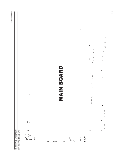
                     8 Wiring Diagrams


8 Wiring Diagram
8-1 Wiring Diagram


                                   8-1
8 Wiring Diagrams

8-2 Main Board Layout (40"/46")


                                     LVDS (30P)


                                                                                                                              Sound
                     Inverter       DDR                                                                                        amp
                     Control
                       (5P)
                                                    SVP-LX

                                    DDR


                                                                                                                              Sound
                                    main                                                                                      Block
                      Power
                                   micom
                      (32P)

                                                                                                             TUNER
                                                                                                             BLOCK


                    Deburgging      Sub                      HDMI-IC
                       (5P)        micom


                                                                 JA300
                      Sub
                     micom
                      (5P)


                                                                  CN300      CN301
                                 CN201_NT


                                                                 JA301          JA302                JA210           JA209
                                 JA201_NT

                                                                   CN900         CN101       CN102     CN200          CN305
                                                                   (15P)          (3P)        (2P)     (14P)          (16P)
                      JA204                 JA205                  Control           Speaker Jack     Side AV          MMS


8-2
                                                                                                                              8 Wiring Diagrams

8-3 Main Board Layout (52")


                                 LVDS (24P)
                   LVDS
                   (20P)


                                                                                                                      Sound
                   Power         DDR                                                                                   amp
                   (32P)
                                                 SVP-LX

                                 DDR


                                  main
                                 micom                                                                                Sound
                  Inverter                                                                                            Block
                  Control
                    (5P)
                                                                                                      TUNER
                                                                                                      BLOCK


                 Deburgging      Sub                  HDMI-IC
                    (5P)        micom


                                                          JA300
                    Sub
                   micom
                    (5P)


                                                           CN300      CN301


                              CN201_NT


                                                          JA301          JA302                JA210           JA209
                              JA201_NT

                                                            CN900         CN101       CN102     CN200
                                                            (15P)          (3P)        (2P)     (14P)
                   JA204                 JA205              Control           Speaker Jack     Side AV


                                                                                                                                            8-3
8 Wiring Diagrams

8-4 PIN characteristic

CN100 - Main Board power supply

      PIN            1         2       3        4       5         6       7          8     9       10         11     12     13     14    15        16
      NAME          SW       GND     GND      GND     GND        A5V     A5V        A5V   A5V     A5V         GND   GND    B12VS B12VS   GND       GND
               POWER


      PIN           17        18      19       20      21        22      23         24    25       26         27     28     29     30    31        32
      NAME          GND      GND     B5V      B5V     B5V        B5V    GND      GND      GND     GND      B12V     B12V   B12V   B12V   GND       GND

  Function Define
        - B12V           B12V_CHN, B9V, B8V, B5V_VCCT
        - B5V            B33V, B5V_VCCA, B3.3VD, B2.5V_VDD, B1.8VD, PX_VD1.8, PX_VA1.8, PX_VL1.8, B1.2VD
        - B12VS          B12VS
        - A5V            A5V_1, A3.3V


CN101 / CN102 - SPEAKER CONNECTOR

             PIN                      1                     2                   3                       PIN                1                  2
           NAME                      R+                     NC                 R-                    NAME                  L+                 L-


8-4
                                                                                                                                     8 Wiring Diagrams

CN900 - Front control

    PIN       1         2        3        4         5        6          7    8    9       10      11     12     13      14     15
  NAME SDA-T SCL-T              GND     KEY       LED      GND      A5V     GND   IR     KEY     KEY     GND   IDENT   HP-L   HP-R
                                       INPUT1                                            INPUT1 INPUT2          HP

 Function Define
       - A5V     Front control board poewr supply
       - KEY INPUT1,2 Key control, from the memu, change up/down Etc.
       - IR      Remote control signal
       - LED     Control the timing and stand by LED color


CN505 - Panel control

     PIN                1                 2                  3               4              5
    NAME          SW_inverter        Ana_dimming        PWM_dimming         GND        Sense_Power

 Function Define
       - SW_inverter         panel inverter control, about 3.3V
       - Ana_dimming         panel dimming control
       - PWM_dimming         panel PWM control, duty 40% ~ 90%


                                                                                                                                                   8-5
8 Wiring Diagrams

LVDS Signal (40"/46")

 PIN                   NAME       PIN     NAME
      1                VDD        16    TXOUTO2-
      2                VDD        17    TXOUTO1+
      3                VDD        18    TXOUTO1-
      4                VDD        19    TXOUTIO0+
      5                VDD        20    TXOUTO0-
      6                GND        21    TXOUTE3+
      7                GND        22    TXOUTE3-
      8                GND        23    TXOUTEC+
      9                GND        24    TXOUTEC-
      10            LVDS OPTION   25    TXOUTE2+
      11             TXOUTO3+     26    TXOUTE2-
      12             TXOUTO3-     27    TXOUTE1+
      13             TXOUTOC+     28    TXOUTE1-
      14             TXOUTOC-     29    TXOUTE0+
      15            TXOUTOC2+     30    TXOUTE0-


8-6
                                           8 Wiring Diagrams

LVDS Signal (52")

  PIN           NAME      PIN    NAME
   1                VDD   13    TXOUTO1+
   2                VDD   14    TXOUTO2-
   3                VDD   15    TXOUTO2+
   4                VDD   16      GND
   5                VDD   17    TXOUTOC-
   6            GND       18    TXOUTOC+
   7            GND       19      GND
   8            GND       20    TXOUTO3-
   9            GND       21    TXOUTO3+
  10          TXOUTO0-    22    TXOUTO4-
  11          TXOUTO0+    23    TXOUTO4+
  12          TXOUTO1-    24      GND


  PIN           NAME      PIN    NAME
   1          TXOUTE0-    11    TXOUTE3-
   2          TXOUTE0+    12    TXOUTE3+
   3          TXOUTE1-    13    TXOUTE4-
   4          TXOUTE1+    14    TXOUTE4+
   5          TXOUTE2-    15      GND
   6          TXOUTE2+    16      NC
   7            GND       17      NC
   8          TXOUTEC-    18      NC
   9         TXOUTEC+     19      NC
  10            GND       20      NC


                                                         8-7
8 Wiring Diagrams

8-5 Power Board Layout


                                     CNM803 14PIN                CNM802 14PIN

                                               Inverter power supply


                    Line Filter                                                     Multi


                          1                                                           3


                                                                                  Main Board
                                                                                 Power supply


                                    Stand By


                                       2


                         AC Input   Stand By                       Main Board                    Panel
                                                                  Power supply                  Control
                         CN801
                                                                 CNM801 16PIN                   CNI804


8-8
                                                                                                                                    8 Wiring Diagrams

CN801 - AC Input

             PIN                              I                         2
            NAME                            Live                   Netural
          VOLTAGE                            AC                     AC
 Functing Define
       - Refer to : AC Input


CN801 - Main Board power supply

    PIN         1          2        3        4        5        6     7        8     9      10        11    12    13    14     15          16
  NAME        13V       GND       5.4V      5.4V   5.4V      GND   GND       GND   12V     12V       12V   GND   GND   GND   ST7V       PWR

 Functing Define
       - ST7V Stand-By Output
       - PWR Power On/Off Control

       - Refer to : CN801 function define

CNM804 - Panel control

     PIN                 1                   2                 3              4                  5
   NAME             SW_inverter         Ana_dimming       PWM_dimming        GND         SENSOR POWER

 Functing Define
       - Refer to : CN815 function define


                                                                                                                                                  8-9
8 Wiring Diagrams

CN802 - Inverter power supply

       PIN           1          2       3           4    5     6     7     8     9    10    11    12    13    14
       NAME         24V       24V      24V      24V     24V   GND   GND   GND   GND   GND   GND   B/L   A_D   P_D
  Functing Define
        - AMLCD           Panel Inverter Power
        - 24V             LAMP INVERTER Voltage
        - B/L             Brightness sensor power
        - A_D             ANA_DIMMING
        - P_D             PWM_DIMMING


CN803 - Inverter power supply

       PIN           1          2       3           4    5     6     7     8     9    10    11    12    13    14
       NAME         24V       24V      24V      24V     24V   GND   GND   GND   GND   GND   A_D   B/L   P_D   GND
  Functing Define
        - AUO             Panel Inverter Power
        - 24V             LAMP INVERTER Voltage
        - B/L             Brightness sensor power
        - A_D             ANA_DIMMING
        - P_D             PWM_DIMMING


8-10
                                                                                    8 Wiring Diagrams


                CN804 14PIN                CN803 14PIN

                         Inverter power supply


Line Filter                                                   Multi


    1                                                           3


                                                            Main Board
                                                           Power supply


              Stand By


                 2


  AC Input    Stand By                       Main Board                    Panel
                                            Power supply                  Control
   CN800
                                            CN801 16PIN                   CN802


                                                                                                8-11
8 Wiring Diagrams

CN801 - AC Input

                    PIN                           I                          2
               NAME                              Live                   Netural
             VOLTAGE                             AC                      AC
  Functing Define
        - Refer to : AC Input


CN801 - Main Board power supply

       PIN           1         2         3        4        5        6     7        8     9      10    11     12    13    14     15    16
       NAME         13V       GND       5.4V    5.4V    5.4V      GND   GND       GND   12V     12V   12V    GND   GND   GND   ST7V   PWR

  Functing Define
        - ST7V Stand-By Output
        - PWR Power On/Off Control

          - Refer to : CN801 function define

CNM804 - Panel control

        PIN                    1                  2                 3              4              5
       NAME               SW_inverter        Ana_dimming       PWM_dimming        GND         SENSOR POWER

  Functing Define
        - Refer to : CN815 function define


8-12
                                                                                                             8 Wiring Diagrams

CN803 - Inverter power supply

    PIN        1         2       3           4    5     6     7     8     9    10    11    12    13    14
  NAME       24V       24V      24V      24V     24V   GND   GND   GND   GND   GND   GND   B/L   A_D   P_D
 Functing Define
       - AMLCD     Panel Inverter Power
       - 24V       LAMP INVERTER Voltage
       - B/L       Brightness sensor power
       - A_D       ANA_DIMMING
       - P_D       PWM_DIMMING


CN804 - Inverter power supply

    PIN        1         2       3           4    5     6     7     8     9    10    11    12    13    14
  NAME       24V       24V      24V      24V     24V   GND   GND   GND   GND   GND   B/D   P_L   GND   B/L
 Functing Define
       - CMO       Panel Inverter Power
       - 24V       LAMP INVERTER Voltage
       - B/L       Brightness sensor power
       - P_D       PWM_DIMMING


                                                                                                                         8-13
8 Wiring Diagrams

Memo


8-14


◦ Jabse Service Manual Search 2024 ◦ Jabse PravopisonTap.bg ◦ Other service manual resources online : FixyaeServiceinfo