Service Manuals, User Guides, Schematic Diagrams or docs for : Samsung LCD TV LE26R71B 14_Wiring Diagram
<< Back | HomeMost service manuals and schematics are PDF files, so You will need Adobre Acrobat Reader to view : Acrobat Download Some of the files are DjVu format. Readers and resources available here : DjVu Resources
For the compressed files, most common are zip and rar. Please, extract files with Your favorite compression software ( WinZip, WinRAR ... ) before viewing. If a document has multiple parts, You should download all, before extracting.
Good luck. Repair on Your own risk. Make sure You know what You are doing.
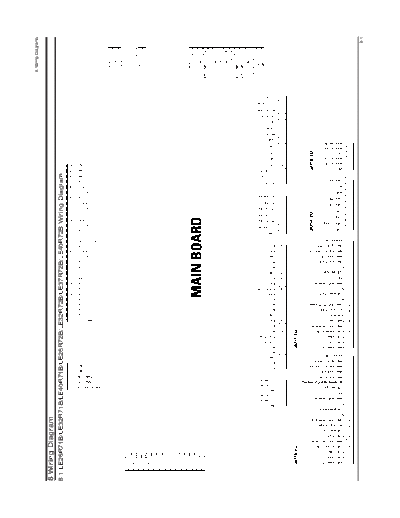
Image preview - the first page of the document

>> Download 14_Wiring Diagram documenatation <<
Text preview - extract from the document
                                                                                    8 Wiring Diagrams


8 Wiring Diagram
8-1 LE26R71B/LE32R71B/LE40R71B/LE26R72B/LE32R72B/LE37R72B/LE40R72B Wiring Diagram


                                                                                                  8-1
8 Wiring Diagrams

8-2 Main Board Layout


8-2
                                                                                                                                8 Wiring Diagrams

8-3 PIN characteristic

CN800 - Main Board power supply

   PIN         1         2        3         4         5          6     7         8   9   10         11   12   13    14    15          16
  NAME B12V            GND      B5V       B5V       B5V         GND   GND    GND B12VS B12VS B12VS GND        GND   GND   A5V       A5V
 Function Define
       - B12V      B8V, B5V-T
       - B5V       B5V-1, B5V, 5V-P, B1.8V
       - B12VS     B12VS
       - A5V       A5V, A3.3V-3, A3.3V, A3.3V-1, B3.3V, A1.8V


CN600 / CN601 - SPEAKER CONNECTOR

         PIN                     1                        2                 3                 PIN             1                2
       NAME                     R+                        NC                R-            NAME                L+               L-


                                                                                                                                              8-3
8 Wiring Diagrams

CN221 - Front control

      PIN           1        2        3       4        5         6       7             8   9     10     11      12    13   14   15
      NAME SDA-T SCL-T GND                   KEY     LED       GND     A5V       GND       IR   KEY     KEY     GND IDENT HP-L HP-R
                                            INPUT1                                              INPUT1 INPUT2        HP
  Function Define
        - A5V     Front control board poewr supply
        - KEY INPUT1,2/SDA/SCL       Key control, from the memu, change up/down Etc.
        - IR      Remote control signal
        - LED     Control the timing and stand by LED color


CN501 - Panel control

        PIN                 1                 2                  3                     4           5
       NAME             SW_inverter       Ana_dimming PWM_dimming                GND              GND
  Function Define
        - SW_inverter            panel inverter control, about 3.3V
        - Ana_dimming            panel dimming control
        - PWM_dimming            panel PWM control, duty 40% ~ 90%


8-4
8 Wiring Diagrams


              8-5
8 Wiring Diagrams

8-4 Power Board Layout


8-6
                                                                                                                             8 Wiring Diagrams

CN801 - AC Input

             PIN                              I                   2
           NAME                             Live                Netural
        VOLTAGE                              AC                  AC
 Functing Define
       - Refer to : AC Input


CN801 - Main Board power supply

   PIN          1          2        3        4      5      6      7        8     9      10       11    12    13    14   15         16
  NAME        13V       GND 5.4V            5.4V   5.4V   GND   GND       GND   12V    12V       12V   GND   GND   GND ST7V PWR
 Functing Define
       - ST7V Stand-By Output
       - PWR Power On/Off Control

       - Refer to : CN801 function define

CNM804 - Panel control

     PIN                 1                   2             3               4                 5
    NAME            SW_inverter         Ana_dimming PWM_dimming           GND         SENSOR POWER
 Functing Define
       - Refer to : CN815 function define


                                                                                                                                           8-7
8 Wiring Diagrams

CN802 - Inverter power supply

      PIN            1          2       3           4    5     6     7     8   9    10    11    12    13    14
      NAME          24V       24V     24V       24V     24V   GND   GND   GND GND   GND   GND   B/L   A_D   P_D
  Functing Define
        - AMLCD           Panel Inverter Power
        - 24V             LAMP INVERTER Voltage
        - B/L             Brightness sensor power
        - A_D             ANA_DIMMING
        - P_D             PWM_DIMMING


CN803 - Inverter power supply

      PIN            1          2       3           4    5     6     7     8   9    10    11    12    13    14
      NAME          24V       24V     24V       24V     24V   GND   GND   GND GND   GND   A_D   B/L   P_D   GND
  Functing Define
        - AUO             Panel Inverter Power
        - 24V             LAMP INVERTER Voltage
        - B/L             Brightness sensor power
        - A_D             ANA_DIMMING
        - P_D             PWM_DIMMING


8-8
8 Wiring Diagrams


              8-9
8 Wiring Diagrams

CN801 - AC Input

                    PIN                          I                   2
               NAME                            Live                Netural
            VOLTAGE                             AC                  AC
  Functing Define
        - Refer to : AC Input


CN801 - Main Board power supply

       PIN           1        2        3        4      5      6      7        8     9      10   11      12   13    14   15   16
   NAME             13V      GND 5.4V          5.4V   5.4V   GND   GND       GND   12V    12V   12V   GND    GND   GND ST7V PWR
  Functing Define
        - ST7V Stand-By Output
        - PWR Power On/Off Control

          - Refer to : CN801 function define

CNM804 - Panel control

        PIN                  1                  2             3               4             5
       NAME              SW_inverter       Ana_dimming PWM_dimming           GND         SENSOR POWER
  Functing Define
        - Refer to : CN815 function define


8-10
                                                                                                           8 Wiring Diagrams

CN803 - Inverter power supply

    PIN        1         2       3           4    5     6     7     8   9    10    11    12    13    14
  NAME       24V       24V     24V       24V     24V   GND   GND   GND GND   GND   GND   B/L   A_D   P_D
 Functing Define
       - AMLCD     Panel Inverter Power
       - 24V       LAMP INVERTER Voltage
       - B/L       Brightness sensor power
       - A_D       ANA_DIMMING
       - P_D       PWM_DIMMING


CN804 - Inverter power supply

    PIN        1         2       3           4    5     6     7     8   9    10    11    12    13    14
  NAME       24V       24V     24V       24V     24V   GND   GND   GND GND   GND   B/D   P_L   GND   B/L
 Functing Define
       - CMO       Panel Inverter Power
       - 24V       LAMP INVERTER Voltage
       - B/L       Brightness sensor power
       - P_D       PWM_DIMMING


                                                                                                                       8-11
8 Wiring Diagrams

Memo


8-12
◦ Jabse Service Manual Search 2024 ◦ Jabse Pravopis ◦ onTap.bg ◦ Other service manual resources online : Fixya ◦ eServiceinfo