Service Manuals, User Guides, Schematic Diagrams or docs for : Samsung LCD TV LE32R88BD LE23R86BD_SB-ET-EX-SI_4728966536
<< Back | HomeMost service manuals and schematics are PDF files, so You will need Adobre Acrobat Reader to view : Acrobat Download Some of the files are DjVu format. Readers and resources available here : DjVu Resources
For the compressed files, most common are zip and rar. Please, extract files with Your favorite compression software ( WinZip, WinRAR ... ) before viewing. If a document has multiple parts, You should download all, before extracting.
Good luck. Repair on Your own risk. Make sure You know what You are doing.
Image preview - the first page of the document
>> Download LE23R86BD_SB-ET-EX-SI_4728966536 documenatation <<
Text preview - extract from the document
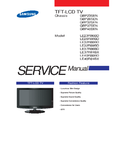
TFT-LCD TV
Chassis GBP23SEN
GBP26SEN
GBP32SEN
GBP37SEN
GBP40SEN
Model LE23R86BD
LE26R88BD
LE32R88BD
LE32R89BD
LE37R86BD
LE37R81BX
LE40R88BD
LE40R81BX
SERVICE Manual
TFT-LCD TV Fashion Feature
- Luxurious Slim Design
- Supreme Picture Quality
- Supreme Sound Quality
- Supreme Convenience Quality
- Convenience for Users
- iDTV
Copyright Trademarks
2007 by Samsung Electronics Co., Ltd. Samsung is the registered trademark of Samsung
Electronics Co., Ltd.
All rights reserved.
LE23R86BD/LE26R88BD/LE32R88BD/
This manual may not, in whole or in part, be copied, LE37R86BD/LE40R88BD Service Manual and
photocopied, reproduced, translated, or converted to any Macmaster Cable Adapter are trademarks of Samsung
electronic or machine readable form without prior Electronics Co., Ltd.
written permission of Samsung Electronics Co., Ltd.
Macintosh and Power Macintosh are trademarks of
LE23R86BD/LE26R88BD/LE32R88BD/
Apple Computer, Inc.
LE37R86BD/LE40R88BD Service Manual
All other trademarks are the property of their respective
First edition March 2007.
owners.
Printed in Korea.
ii
Contents
1. Precautions .........................................................................................................................................................1-1
1
1-1 Safety Precautions ....................................................................................................................................... 1-1
1-2 Servicing Precautions .................................................................................................................................... 1-2
1-3 Static Electricity Precautions ........................................................................................................................... 1-2
1-4 Installation Precautions.................................................................................................................................... 1-3
2. Product specifications ..........................................................................................................................................2-1
2
2-1 Fashion Feature ............................................................................................................................................. 2-1
2-2 LE23R86BD Specifications .............................................................................................................................. 2-2
2-3 LE26R86BD Specifications .............................................................................................................................. 2-3
2-4 LE32R86BD Specifications .............................................................................................................................. 2-4
2-5 LE37R86BD Specifications .............................................................................................................................. 2-5
2-6 LE40R86BD Specifications .............................................................................................................................. 2-6
2-7 Spec Comparison .......................................................................................................................................... 2-7
2-8 Option Specification ....................................................................................................................................... 2-8
3. Alignments and Adjustments .................................................................................................................................3-1
3
3-1 Service Instruction ....................................................................................................................................... 3-1
3-2 How to Access Service Mode ........................................................................................................................... 3-2
3-3 Factory Data ................................................................................................................................................ 3-3
3-4 Service Adjustment ....................................................................................................................................... 3-11
3-5 Software Upgrade ....................................................................................................................................... 3-14
4. Troubleshooting ................................................................................................................................................4-1
4
4-1 First Checklist for Troubleshooting .....................................................................................................................4-1
4-2 Checkpoints by Error Mode .............................................................................................................................. 4-2
5. Exploded View and Parts List .................................................................................................................................5-1
5
5-1 LE23R86BD Exploded View ..............................................................................................................................5-1
5-2 LE23R86BD Parts list .................................................................................................................................... 5-2
5-3 LE26R88BD Exploded View ........................................................................................................................... 5-3
5-4 LE26R88BD Parts list .................................................................................................................................... 5-4
5-5 LE32R88BD Exploded View ........................................................................................................................... 5-5
5-6 LE32R88BD Parts list .................................................................................................................................... 5-6
5-7 LE37R86BD Exploded View ........................................................................................................................... 5-7
5-8 LE37R86BD Parts list .................................................................................................................................... 5-8
5-9 LE40R88BD Exploded View ........................................................................................................................... 5-7
5-10 LE40R88BD Parts list .................................................................................................................................... 5-8
Contents
6. Electrical Parts List .............................................................................................................................................6-1
6
6-1 LE32R88BDX Parts List ................................................................................................................................. 6-1
7. Block Diagram ...................................................................................................................................................7-1
7
8. Wiring Diagram ...................................................................................................................................................8-1
8
8-1Wiring Diagram................................................................................................................................................8-1
8-2 Main Board Layout ....................................................................................................................................... 8-2
8-3 PIN characteristic .......................................................................................................................................... 8-3
8-4 Connector Location and PCB outline figure ......................................................................................................... 8-6
8-5 Output Connector .......................................................................................................................................... 8-7
9. Schematic Diagrams .............................................................................................................................................9-1
9
10. Operating Instructions and Installation.....................................................................................................................10-1
1
10-1 Front ...................................................................................................................................................... 10-1
10-2 Viewing the Connection Panel ..................................................................................................................... 10-2
10-3 Remote control .......................................................................................................................................... 10-5
10-4 Installation the Stand ................................................................................................................................. 10-6
10-5 Installing the Wall Mount Kit ........................................................................................................................ 10-6
11. Disassembly and Reassembly ..............................................................................................................................11-1
1
11-1 Disassembly ............................................................................................................................................. 11-1
11-2 Reassembly ............................................................................................................................................. 11-5
12. PCB Diagram ...................................................................................................................................................12-1
1
12-1 Main PCB Diagram (Without Card Slot) ......................................................................................................... 12-1
12-2 Main PCB Diagram (With Card Slot) ...............................................................................................................12-2
13. Circuit Descriptions .............................................................................................................................................13-1
1
13-1 Main Signal Description .............................................................................................................................. 13-1
13-2 DTV Signal Description .............................................................................................................................. 13-2
13-3 RF/DTV Tuner (DNOS403MH261B(S)) SPEC. ................................................................................................ 13-3
13-4 DTV MAIN ChipSet .................................................................................................................................... 13-9
14. Reference Infomation ....................................................................................................................................... 14-1
14-1 Technical Terms ....................................................................................................................................... 14-1
14-2 Pin Assignments ....................................................................................................................................... 14-4
14-3 Timing Chart ............................................................................................................................................. 14-7
14-4 Panel Description .................................................................................................................................... 14-11
Samsung Electronics Co.,Ltd.
- This Service Manual is a property of 416, Maetan-3Dong, Yeongtong-Gu, Suwon City,
Samsung Electronics Co., Ltd. Gyeonggi-Do, Korea, 443-742
Any unauthorized use of Manual can be Printed in Korea
punished under applicable International P/N : BN82-00183B-00
and/or domestic law. URL : http://itself.sec.samsung.co.kr/
13 Circuit Descriptions
13 Circuit Descriptions
13-1 Block description
Signal
Power
IP Board
RF IN
Scart 1,2
A/V
S-Video Main
Board Panel
Component T-con
Board
HDMI 1, 2
PC
Speaker
IR/LED
Bordeaux consists of three main blocks
1. Main board : Video signal processing
2. IP board : Power supply & Inverter
3. T-con board : LCD Panel control
13-1
13 Circuit Descriptions
Signal
Power SMPS INVERTER
RF IN
Scart 1,2
A/V
S-Video Main
Board Panel
Component T-con
Board
HDMI 1, 2
PC
Speaker
IR/LED
Bordeaux consists of three main blocks
1. Main board : Video signal processing
2. SMPS : Power supply
3. T-con board : LCD Panel control
13-2
13 Circuit Descriptions
13-2 Main Block
13-3
13 Circuit Descriptions
13-3 SMPS Board
13-3-1 23" Power Block
Line PFC Inverter
Resonance
Filter AC Switching PFC Resonance SMPS
Switching
Part Rectifier Part Rectifier Transformer Output 24V
Part
Rectifier
Part Signal
DC/DC
MC33167 5.3V
AC Input PFC Resonance
(90Vac~264Vac) Controler Controller
Signal
TDA4863 MC33067
13V
Regulator Sound
On/Off KA78R09 12V
Control
On/Off
Stand-By
Controller Output
ST-BY Stand-By
VIPer12A Rectifier
Transformer 5.2V
Part
13-3-2 23" SMPS Diagram
PFC PFC DC Current
Rectifier Output Resonant Type Trans EER3944
EMI INVERTER
FILTER 24V
INPUT
450V
AC Input 150uF
90V~264V TDA4863 Main
+13V
F222L Regulator
Sound
+9V
Trans EE2020
DC/DC V5D
Converter +5.3V
VIPer12A
Stand-By
5.2V
On/Off Power On/Off
Control Signal
13-4
13 Circuit Descriptions
Output Voltage Output Current
Output
Load Characteristics PCB Loc. Usage Remark
Name
Normal Regulation(%) Variable Range Min Typical Peak
24V 24.5V ◦ Jabse Service Manual Search 2024 ◦ Jabse Pravopis ◦ onTap.bg ◦ Other service manual resources online : Fixya ◦ eServiceinfo