Service Manuals, User Guides, Schematic Diagrams or docs for : Samsung LCD TV LE37S73BD 10_Wiring Diagram

<< Back | Home

Most service manuals and schematics are PDF files, so You will need Adobre Acrobat Reader to view : Acrobat Download Some of the files are DjVu format. Readers and resources available here : DjVu Resources
For the compressed files, most common are zip and rar. Please, extract files with Your favorite compression software ( WinZip, WinRAR ... ) before viewing. If a document has multiple parts, You should download all, before extracting.
Good luck. Repair on Your own risk. Make sure You know what You are doing.


Image preview - the first page of the document
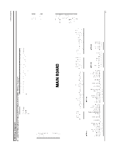
10_Wiring Diagram


>> Download 10_Wiring Diagram documenatation <<

Text preview - extract from the document
                                                             8 Wiring Diagrams


8 Wiring Diagram
8-1 LE27S73BD/LE32S73BD/LE37S73BD/LE40S73BD Wiring Diagram


                                                                           8-1
8 Wiring Diagrams

8-2 Main Board Layout


                                                          CN4004 30PIN                                 CN5002 34PIN                       CN5003 34PIN
                                                            LVDS JACK                               DTV Module Connector


                                                                                         MAIN                                                                    AMP
                                                CONTROL
                    CN402


                                                                                        MICOM
                                 PANEL


                                                                                                                                                             SOUND BLOCK


                                                                                                                                                               STV 8257
                                 POWER SUPPLY
                    CN10016PIN


                                                                                                    SVP-PX56
                                                                                                     BLOCK

                                                                                                                                  TUNER
                                                                 SUB                                                              BLOCK
                                                                MICOM


                                                                                                              CN5001 15PIN   CN1002   CN1003     CN2002_32
                                                                JA714_OP        JA712_OP JA717_OP
                                                                           Option 26"                            Function      SPEAKER JACK       CONTROL


8-2
                                                                                                                                8 Wiring Diagrams

8-3 PIN characteristic

CN1001 - Main Board power supply

    PIN         1        2      3       4      5          6     7         8    9    10         11   12      13    14      15          16
  NAME      B12V       GND     B5V    B5V     B5V        GND   GND       GND B12VS B12VS B12VS      GND    GND    GND     A5V        A5V

 Function Define
       - 12V        B5V_VCCA, B5V_VCCB, IC611 POWER SUPPERLY
       - 5V         B5V, B3.3V, B2.5V_VDD, B3.3VD, VCC50
       - 12VS       B12VS


CN1002 / CN1003 - SPEAKER CONNECTOR

          PIN                  1                    2                3                   PIN                1                   2
       NAME                  R-OUT                 NOP         R-REFERENCE            NAME                L-OUT         L-REFERENCE


                                                                                                                                              8-3
8 Wiring Diagrams

CN5001 - Front control

      PIN            1        2         3       4         5       6       7            8   9      10        11      12    13    14    15
      NAME          GND      GND       A5V       -     KEY       KEY   GND             -   IR     -        LED_    LED_   GND   SDA   SCL
                                                      INPUT1 INPUT2                                        GREEN   LED

  Function Define
        - A5V     Front control board poewr supply
        - KEY INPUT1,2/SDA/SCL       Key control, from the memu, change up/down Etc.
        - IR      Remote control signal
        - LED_GREEN/LED_RED          Control the timing and stand by LED color


CN4002 - Panel control

        PIN                   1                  2                 3                   4               5
      NAME               SW_inverter        Ana_dimming       PWM_dimming        GND            SENSOR POWER

  Function Define
        - SW_inverter              panel inverter control, about 5V
        - Ana_dimming              panel dimming control
        - PWM_dimming              panel PWM control, duty 40% ~ 90%
        - SENSOR POWER             brightness sensor power supply


8-4
                                                 8 Wiring Diagrams

CN4004 - LVDS Signal


  PIN            NAME        PIN      NAME
   1             VCC         16    TXOUTCLK +
   2            VCC5P        17     TXOUTCLK -
   3            VCC5P        18        GND
   4            VCC5P        19     TXOUT2 +
   5            VCC5P        20      TXOUT2 -
   6             GND         21        GND
   7             GND         22     TXOUT1 +
   8         NOP (NOT USE)   23      TXOUT1 -
   9             SDA 1       24        GND
   10            SCL 1       25     TXOUT0 +
   11       PANEL_SYNC_EN    26      TXOUT0 -
   12            GND         27        GND
   13          TXOUT3 +      28    SW_INVERTER
   14          TXOUT3 -      29    ANA_DIMMING
   15            GND         30    PWM_DIMMING


                                                               8-5
8 Wiring Diagrams

8-4 Power Board Layout


                                        CNI802 14PIN                         CNI801 14PIN

              CNB806                                   LAMP power supply

               AC input


                                                       LAMP power inverter


                                                                 4                                          Multi
                          Line filter


                              1                                                                               5


                                                                                                        Main Board
                                                                                                       Power supply


                                                                 3


                                                                PFC
                          Stand By                     Power factor correction
                                                            (IC control)


                              2


                                                                                              Main Board              Panel
                          Stand by                                                           Power supply             Control

                          CNB811                                                            CNM801 14PIN              CNI804


8-6
                                                                                                                             8 Wiring Diagrams

CNB811 - Stand by supply

             PIN                             I                          2                  3
           NAME                             Live                   Netural              SW_POWER
          VOLTAGE                           AC                      AC                   ON/OFF
 Functing Define
       - Refer to : CN802 function define


CNM801 - Main Board power supply

    PIN        1          2         3        4        5        6     7        8     9      10        11    12    13    14
 NAME         12V       GND        5V       5V     5V        GND   GND       GND   12V     12V       12V   GND   GND   GND

 Functing Define
       - Refer to : CN801 function define


CNM804 - Panel control

     PIN                 1                   2                 3              4                  5
   NAME            SW_inverter          Ana_dimming       PWM_dimming        GND         SENSOR POWER

 Functing Define
       - Refer to : CN815 function define


                                                                                                                                           8-7
8 Wiring Diagrams

CN801 - Main Board power supply

      PIN            1          2       3           4    5     6     7     8     9    10    11    12    13    14
      NAME          24V       24V      24V      24V     24V   GND   GND   GND   GND   GND   GND   B/L   A_D   P_D
  Functing Define
        - 24V             LAMP INVERTER Voltage
        - B/L             Brightness sensor power
        - A_D             ANA_DIMMING
        - P_D             PWM_DIMMING


8-8


◦ Jabse Service Manual Search 2024 ◦ Jabse PravopisonTap.bg ◦ Other service manual resources online : FixyaeServiceinfo