Service Manuals, User Guides, Schematic Diagrams or docs for : Samsung Plasma D72A chassis Circuit Description
<< Back | HomeMost service manuals and schematics are PDF files, so You will need Adobre Acrobat Reader to view : Acrobat Download Some of the files are DjVu format. Readers and resources available here : DjVu Resources
For the compressed files, most common are zip and rar. Please, extract files with Your favorite compression software ( WinZip, WinRAR ... ) before viewing. If a document has multiple parts, You should download all, before extracting.
Good luck. Repair on Your own risk. Make sure You know what You are doing.
Image preview - the first page of the document
>> Download Circuit Description documenatation <<
Text preview - extract from the document
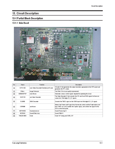
Circuit Description
13. Circuit Description
13-1 Partial Block Description
13-1-1 Main Board
No Name Function Description
A Scaler IC that generates the output resolution appropriate to the PDP panel and
SVP-EX62 main Video Decorder+Deinterlacer+Scaler
generates the PIP screen.
DNIe-L Image Enhancer The DNIe IC for visual quality improvement.
M30620SPGP main Micom Generates various control signals required for operating the circuit.
The Video Decoder IC that converts the Y/C and Scart RGB signals for the main
SAA7119 sub Video Decorder
screen into 10 bit digita R, G, B signals.
SIL9993 HDMI Decorder Converts the TMDS signal on the HDMI input into 8 bit digital R, G, B signals
Detects the Power on/off signal from the remote control and the Power button and
S3F8668 sub Micom turns SMPS on or off, handles the Caption signal, and controls the signal for the
LEDs on the front panel.
MSP4410G Sound processor Sound Processing IC
NSP6241 Sound Effect chip Sound PWM IC
TMQZ6-405A Tuner Tuner CH Tuning and CVBS, SIF
Samsung Electronics 13-1
Circuit Description
13-1-2 Power Button Board
(1) RM01: Remote Control Sensor.
(2) SW001: Power button
(3) OP001: The Illumination sensor that senses the quantity
of light. It senses the illumination and automati
cally adjusts the screen brightness according to
the surrounding brightness when the Power
Saving Mode of the User menu is set to Auto.
13-1-3 Function Key Board
Function Key. Located on the side of the unit.
13-2 Samsung Electronics
Circuit Description
13-2-4 Main SMPS
(1) CN800: AC IN (90 ~ 264V)
(2) (3) (4) (5)
CN804-2 CN803(MAIN SMPS) CN810(Main SMPS) CN809(Main SMPS)
(MAIN SMPS)
CN108(READY B'D) CN2013(Logic B'D) CN3(DC-DC SMPS)
CN109(READY B'D) Pin No Signal Pin No Signal Pin No Signal
Pin No Signal 1 RTN 1 5.3V 1 5.3V
1 FAN-D 2 VT(33V) 2 5.3V 2 Vg
2 FAN-ON 3 RTN_AMP 3 RTN 3 RTN
3 STB5V 4 RTN_AMP 4 RTN 4 RTN
4 RTN 5 18V_AMP 5 5.3V 5 RTN
5 PS-ON 6 18V_AMP 6 RTN 6 RTN
6 12V 7 RTN 7 PS-ON 7 RTN
7 RTN 8 12V 8 N.C 8 Va
8 RTN 9 RTN 9 VS-ON 9 Va
9 VCA 10 6V 10 STB 5V 10 N.C
10 VCS 11 Vs
11 RTN 12 Vs
12 5.3V
13 RTN
14 5.3V
CN811, CN806, CN807 and CN808 are not used.
Samsung Electronics 13-3
Circuit Description
1. Outline (PDP 42inch/50inch SMPS)
Considering various related conditions, the switching regulator with good efficiency and allowing for its small size and light weight
was used as the power supply for PDP 42inch(Schubert)/50inch(Strauss), VS requiring high power consumption Asymmetrical Half
Bridge converter and flyback converter. To comply with the international harmonics standards and improve the power factor, active
PFC(Power Factor Correction) was used to rectify AC input into +400V DC output, which in turns used as input to the switching
regulator.
2. Input
The power supply shall be capable of supplying full rated output power over free voltage ranges that are rated 100 VAC - 240 VAC
RMS nominal. Operating voltage : 90 VAC - 264 VAC
The power supply must be able to start up under peak loading at 90V AC. The power supply shall automatically recover from AC
power loss. (Note that nominal voltages for test purposes are considered to be with +/- 1.0V of nominal).
STD_5V & Vpr2(3.3V) is a SELV standby voltage that is always present when AC mains voltage present.
3. Output
Output Name Output Voltage Output Current(Max.) Using in PDP Driving
VS +190V ~ 220V (210V) 2.0A Sustain Voltage of Drive Board
VA +60V ~ 80V (70V) 3.0A Address Voltage of Drive Board
D5.3V +5.3V 5.0A
A6.5V +6.5V 3.0A
FAN_9V +9V 0.2A
VG +15V 1.0A
D12V +12V 1.5A
A12V +5.3V 0.5A
18VAMP +18V 2.5A Amp Voltage of Audio Board
VT +33V 0.006A
STD_5V +5V 1.0A Standby for Remote Control
4. Over Voltage Protection
The over voltage sense circuitry and reference shall reside in package that are separate and distinct from the regulator control
circuitry and reference. No single point fault shall be able to cause a sustained over voltage condition on any of all outputs.
The supply shall provide latch-mode Over Voltage Protection as defined below.
Parameter Min Unit
VS(210V) 250 ~ V
VA(70V) 100 ~ V
VCC(+5.3V) 6.8 ~ V
5. Short Circuit and Over current Protection
An output short circuit is defined as output impedance of less than 300mohms. The power supply shall shutdown and latch off for
shorting VS DC rails to return. Shorts between main output rails and STD_5V shall not cause any damages to the power supply.
The power supply shall either shutdown and latch off for shorting is removed, the P/S shall recover. The power supply shall be
capable of withstanding a continuous short-circuit to the output without damage or over stress to the unit (components, PCB
traces,connectors,etc.) under the input conditions specified in Section 3 above. Current Protection as defined below.
Output Over Current Limit Unit
VS(210V) 20A, Constant Current.(TBD) A
VA(70V) 10A, Constant Current.(TBD) A
Output except Vs,Va No damage (Auto Recovery or Shut down.) A
13-4 Samsung Electronics
Circuit Description
6. Troubleshooting
Power ON
Abnormal
STD_5V Check the U101, D108
Normal
Abnormal
PFC Check the U201, Q203, Q204
Normal
Abnormal
VA Check the U501
Abnormal
Multi Check the U601
Normal
Abnormal
VS Check the Q401, Q402
Normal
Check the Other board (Image Board or Driver Board) or Cable.
Samsung Electronics 13-5
Circuit Description
13-1-5 DC-DC SMPS
(1) (4), (5) (2) (3)
CN809(Main SMPS) CN1, CN6 CN2(DC-DC SMPS) CN4(DC-DC SMPS)
(DC-DC SMPS) CN5007(Y B'D) CN4000(X B'D)
CN3(DC-DC SMPS) Pin No Signal Pin No Signal
Pin No Signal CN2501(E-Buffer),
CN2701(G-Buffer) 1 Vs 1 Vs
1 5.3V 2 Vs 2 Vs
Pin No Signal
2 Vg 3 RTN 3 RTN
1 RTN
3 RTN 4 RTN 4 RTN
2 N.C
4 RTN 5 Vset 5 Ve
3 5.3V
5 RTN 6 RTN 6 RTN
4 N.C
6 RTN 7 Vscan 7 RTN
5 Va
7 RTN 8 RTN 8 Vg
8 Va 9 Vg 9 5.3V
9 Va 10 5.3V
10 N.C
11 Vs
12 Vs
(6) D5.3V, Vg, Ve Test Point
(7) Va, Vset, Vscan Test Point
13-6 Samsung Electronics
Circuit Description
1. Block Diagram
Vs Input Part Vscan Output
Rectification
Transformer
Block
Auxiliary
Control
Power
and
Switching Block Feedback
Block
Vset Output
Rectification
Transformer
Block
Control Auxiliary
and Power
Switching Block Feedback
Block
Ve Output
Rectification
Transformer
Block
Control Auxiliary
and Power
Switching Block Feedback
Block
DC DC SMPS receives Vs input (195~215V) from the Main SMPS and the necessary Vscan, Vset and Ve voltages are output to
operate the PDP Module as shown in the block diagram above.
Samsung Electronics 13-7
Circuit Description
13-1-6 PDP Module
No Name Parts Code Description
1 ASSY PDP P-X MAIN BOARD BN96-02038A X Drive Board
2 ASSY PDP P-Y MAIN BOARD BN96-02039A Y Drive Board
3 ASSY PDP P-Y BUFF UPPER BOARD BN96-02040A Y Buffer Upper Board
4 ASSY PDP P-Y BUFF LOWER BOARD BN96-02041A Y Buffer Lower Board
5 ASSY PDP P-LOGIC BOARD BN96-02042A Logic Board
6 ASSY PDP P-ADDRESS E BUFF BOARD BN96-02043A Address E Buffer Board
7 ASSY PDP P-ADDRESS F BUFF BOARD BN96-02044A Address f Buffer Board
13-8 Samsung Electronics
Circuit Description
A name of main part of Logic Board and vocabulary.
1 9
10
5
6
3
4
11 2
7 12 8
Item Name Explanation
The connector to receive the RGB, H, V, DATAEN and DCLK signals that have been LVDS encoded through the
LVDS Connector video board. At present, there are 2 LVDS, both internal and external, and only LVDS will be provided in the final
version of the board.
The LED that shows whether the Sync and Clock signal is properly supplied to the logic board (Normal Status:
Operating Status LED
Blinks at 0.8 second intervals)
I2C Connector The connector for the Key Scan board that checks and controls the 512K data.
512K including the Gamma Table, APC Table, drive waveform timing and other options is saved to internal flash
MICOM(ARM-PROCESSOR)
memory.
Y Connector The connector to output the control signal for the Y drive board.
X Connector The connector to output the control signal for the X drive board.
CN2075(E-Adderss Buffer Connector) The connector to output the address data and the control signal to the E-buffer board.
CN2076(F-Adderss Buffer Connector) The connector to output the address data and the control signal to the F-buffer board.
Power Connector The connector to receive power (5V, 3.3V) for the Logic board.
ASIC CHIP The main processor that generates and outputs the logic drive signal and the address data.
MICOM LOADING 5PIN CONNECTOR The connector to load the Micom drive program. The program is loaded by connecting to the GA-WRITER.
VTOGG TP for V Sync Check
About Logic Board
The Logic Board consists of a Logic Main board, which processes the video signal input through LVDS and creates the address
driver output and XY drive signals, and a Buffer board, which buffers the output signal and outputs the signal to the Address Driver
IC (TCP IC).
Logic Board Function Remark
- Video Signal Processing (W/L, error diffusion, APC)
Logic Main - Outputs the Address Driver Control and Data Signals to the Buffer board.
- Outputs the XY Drive Board Control Signal
E Buffer Board Outputs data and control signals to the bottom left TCP IC.
Buffer Board
F Buffer Board Outputs data and control signals to the bottom right TCP IC.
Samsung Electronics 13-9
Circuit Description
Major Check Points and Waveforms
- The waveform during a Normal Operation
When the PDP set and the Logic Board are properly operating, the Operation Status LED blinks at approximately 0.8 second
interval as shown in Figure 1.
If the set is out of order, check the Operation Status LED first, and check that the output waveform is normal using an
oscilloscope.
Check if the waveform is the same as shown in Figure 2 by connecting the oscilloscope to the No. 12 TP in Figure 1. Check if
the waveform is the same as in Figure 3 by connecting the oscilloscope to the connector that is connected to the Buffer board.
If the measured waveform is different from the following waveforms, the board must be replaced.
To check the waveforms, refer to the following waveform patterns.
Figure 2. Normal V-SYNC Output Waveform Figure 3. Normal Address Data Output Waveform
13-10 Samsung Electronics
Circuit Description
Troubleshooting
There are various problems caused by the Logic Board and these have been classified by the Flow Chart.
- No picture on the screen
Check Power Input
Yes No
Check the Operating Status LED Check the power cord
connectivity.
Yes No
Check to see if MICOM Check the fuse
Check that the internal
is operating properly. No
default is black.
(Using key scan. Address: 0080
Yes Check the Input Voltage Level
0000: Black
MICOM
0001: Full White)
Check the ASIC Downloading
control signal output
Yes
Yes
Check to see if the ADDRESS
DATA output is normal. Check that the data and
control signals between
DDR and ASIC are normal.
- Screen Error
Check the
Operating Status LED
MICOM Downloading Check the Video Board
Yes
Check the Internal Waveform Pattern
Screen Trouble with Screen Trouble with
Discharge Trouble Missing Vertical Lines Missing Horizontal Lines
The Buffer Board and the Logic Check the Drive Y-Buffer Output
Main Address Data Output
Check the Detailed Waveform
Check the Short/Open Defect
of the TCP Part.
Samsung Electronics 13-11
Circuit Description
1. X, Y Control Block
Drive Circuit Definition
The Drive Circuit is a circuit that generates a waveform (high-voltage pulse) for the X and Y electrode group of the panel's external
port so as to control the panel. The high-voltage switching pulse is generated through the combination of the IC HYBRID (Drive
block + IGBT) and FET.
Drive Circuit Mechanism
A picture is displayed on the PDP by applying voltage to the X, Y and ADDRESS electrodes of each pixel according to the appro-
priate condition. The drive waveform applied to 42HD V4 is of the ISSS (ISSS: Interweaving Scan and Selective Sustain with Scan
IC) type and has IDS (InDependent Sustain) in the Scan section unlike the existing ADS. Discharges within a PDP pixel can be
classified into 3 types:
Address Discharge: To form a wall voltage within the pixel by giving information (applying DATA voltage) to the pixel to be lit.
Sustain Discharge: Sustain Discharge is a display section that voluntarily maintains the discharge of the pixels whose wall
voltage has been formed by the Address Discharge. (Optical output for displaying a picture is generated).
Erase Discharge: To selectively perform Address Discharge for each pixel, all pixels on the panel should be in the same status
(the wall electric charge status and space electric charge status must be the same). Therefore, the Erase
Discharge section is an important component for guaranteeing the drive margin, and is implemented by
various methods such as applying a log waveform. However, the current 42HD V4 has adopted a wall voltage
control through an RA (Repeated Auto-quenching) reset that separates the discharge area and performs
switching to perform an efficient erase operation, while the gradient was the same in the RAMP section in the
existing approach.
1) Address Discharge
A discharge that is caused by the difference between the plus electric potential (Va apply voltage of 65~70V + Positive Wall
Charge) of the electrode and the negative electric potential (Applied GND Level + Negative Wall Charge) of the Y electrode. The
Address discharge forms a wall voltage within the pixel to display color (to be discharged) before the Sustain Discharge period.
That is, the pixel whose wall charge has been formed by the Address Discharge forms a Sustain Discharge vis the following
Sustain pulse.
2) Sustain Discharge
A Sustain Discharge is a Self-Sustaining Discharge formed by the accumulation of the electric potential of the Sustain pulse (gen-
erally 200 ~ 210 Volt) alternating over the X and Y electrodes during the sustain period, and the wall charge depending on whether
the pixel has previously been discharged or not. That is, it is controlled by the memory characteristics, one of the basic characteris-
tics of the AC PDP (in that the past operating conditions determine the current status). That is, if a wall voltage exists on the pixel
(if the pixel is on), a discharge is formed again because the applied voltage, which is the sum of the following applied Sustain volt-
age and the wall voltage, is higher than the discharge threshold voltage. If no wall voltage exists on the pixel (if the pixel is off), a
discharge will not occur because the Sustain voltage is not higher than the discharge threshold voltage. The Sustain Discharge
period is the period for generating actual optical output so as to display a picture on the PDP screen.
3) Erase Discharge
The purpose of a Reset (Erase) Discharge is to create uniformity of the wall voltage within all panel pixels. It evens the wall volt-
ages regardless of the Sustain Discharge in the previous stage. The Erase Discharge has to remove the wall voltage introduced by
the Sustain Discharge by supplying ions or electrons by a discharge. When the wall voltage is removed through a discharge, the
time when the reverse polarity is applied to the wall voltage (fine width erasing) is to be limited or ions or electrons are to be sup-
plied by a weak discharge (low voltage erasing) so as to prevent a wall charge in reverse polarity.
There are 2 known weak discharge (low-voltage) erase methods. 1) A log waveform adopted by F company and 2) a weak erase
discharge via a ramp waveform adopted by Matsushita and other companies. Both methods control the externally applied voltage
by the difference of the wall voltage of the pixel by applying the rising gradient of the erasing waveform slowly, because the dis-
charge begins when the sum of the existing remaining wall voltage and the rising waveform voltage exceeds the drive threshold
voltage. In addition, a weak discharge is introduced, because the applied voltage is low.
13-12 Samsung Electronics
Circuit Description
Drive Circuit Operating Block Diagram
- Y Drive Board
Power Input Part
Logic Signal Input Part
Logic Signal Buffer
- X Drive Board
Power Input Part
Logic Signal Input Part
Logic Signal Buffer
Requisite Components Necessary for Drive Board Operation
- Power : Supplied from the power board. The optimal value may differ from the following:
a) Vs : 205V - Sustain
b) Vset : 195V - Y Rising Ramp
c) Ve : 100V - Ve bias
d) Vscan : -190V - Scan low bias
e) Vnf : -175V - Y falling Ramp (Created by the DC-DC power block of the Y Drive board)
f) Vsc_h : -70V - Scan high bias (Created by the DC-DC power block of the Y Drive board)
g) Vdd : 5V - Logic signal buffer IC and IPM
h) Vcc : 15V - Gate drive IC ◦ Jabse Service Manual Search 2024 ◦ Jabse Pravopis ◦ onTap.bg ◦ Other service manual resources online : Fixya ◦ eServiceinfo