Service Manuals, User Guides, Schematic Diagrams or docs for : Samsung Plasma PS42-50C96HDX CH F30A Schematic Diagram
<< Back | HomeMost service manuals and schematics are PDF files, so You will need Adobre Acrobat Reader to view : Acrobat Download Some of the files are DjVu format. Readers and resources available here : DjVu Resources
For the compressed files, most common are zip and rar. Please, extract files with Your favorite compression software ( WinZip, WinRAR ... ) before viewing. If a document has multiple parts, You should download all, before extracting.
Good luck. Repair on Your own risk. Make sure You know what You are doing.
Image preview - the first page of the document
>> Download Schematic Diagram documenatation <<
Text preview - extract from the document
Schematic Diagram
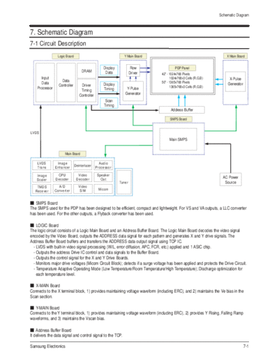
7. Schematic Diagram
7-1 Circuit Description
Logic Board Y Main Board X Main Board
Display Row PDP Panel
DRAM Data Driver 42" - 1024x768 Pixels
Input 1024x768x3 Cells (R,G,B) X-Pulse
Data 50" - 1365x768 Pixels
Data Display Generator
Controller Driver 1365x768x3 Cells (R,G,B)
Processor Timing Y-Pulse
Timing
Controller Generator
Scan
Timing
Address Buffer
SMPS Board
LVDS
Main SMPS
Main Board
LVDS Image Audio
Deinterlacer
Trans Enhancer Processor
Image CPU Video Speaker
Decoder Decoder Out
AC Power
Scaler
Tuner Source
TMDS A/D Video
Converter S/W Micom
Recever
SMPS Board
The SMPS used for the PDP has been designed to be efficient, compact and lightweight. For VS and VA outputs, a LLC converter
has been used. For the other outputs, a Flyback converter has been used.
LOGIC Board
The logic circuit consists of a Logic Main Board and an Address Buffer Board. The Logic Main Board decodes the video signal
encoded by the Video Board, outputs the ADDRESS data signal for each pattern and generates X and Y drive signals. The
Address Buffer Board buffers and transfers the ADDRESS data output signal using TCP IC.
- LVDS with built-in video signal processing (W/L, error diffusion, APC, FCR, etc.) applied and 1 ASIC chip.
- Outputs the address Drive IC control and data signals to the Buffer Board.
- Outputs the control signal for the X and Y Drive Boards.
- Monitors major drive voltages (Micom Circuit Block); detects if a surge voltage has been applied and protects the Drive Circuit.
- Temperature Adaptive Operating Mode (Low Temperature/Room Temperature/High Temperature); Discharge optimization for
each temperature level.
X-MAIN Board
Connects to the X terminal block, 1) provides maintaining voltage waveform (including ERC), and 2) maintains the Ve bias in the
Scan section.
Y-MAIN Board
Connects to the Y terminal block, 1) provides maintaining voltage waveform (including ERC), 2) provides Y Rising, Falling Ramp
waveforms, and 3) maintains the Vscan bias.
Address Buffer Board
It delivers the data signal and control signal to the TCP.
Samsung Electronics 7-1
MEMO
7-2 Samsung Electronics
Schematic Diagram
7-2 Schematic Diagram
7-2-1 Power
This Document can not be used without Samsung's authorization.
Power
Samsung Electronics 7-3
Schematic Diagram
7-2-2 Sound Processing
This Document can not be used without Samsung's authorization.
Power
Samsung Electronics 7-4
Schematic Diagram
7-2-3 Input & Output Jack I
This Document can not be used without Samsung's authorization.
Power
7-5 Samsung Electronics
Schematic Diagram
7-2-4 Input & Output Jack II
This Document can not be used without Samsung's authorization.
Power
Samsung Electronics 7-6
Schematic Diagram
7-2-5 MICOM
This Document can not be used without Samsung's authorization.
Power
7-7 Samsung Electronics
Schematic Diagram
7-2-6 SVP-UX (Scaler)
This Document can not be used without Samsung's authorization.
Power
Samsung Electronics 7-8
Schematic Diagram
7-2-7 DDR & Tuner
This Document can not be used without Samsung's authorization.
Power
7-9 Samsung Electronics
Schematic Diagram
7-2-8 DTV Reset & AV out
This Document can not be used without Samsung's authorization.
Power
Samsung Electronics 7-10
Schematic Diagram
7-2-9 DTV Memory & STi5105
This Document can not be used without Samsung's authorization.
Power
7-11 Samsung Electronics
Schematic Diagram
7-2-10 PCMCIA & STi5105
This Document can not be used without Samsung's authorization.
Power
Samsung Electronics 7-12
◦ Jabse Service Manual Search 2024 ◦ Jabse Pravopis ◦ onTap.bg ◦ Other service manual resources online : Fixya ◦ eServiceinfo