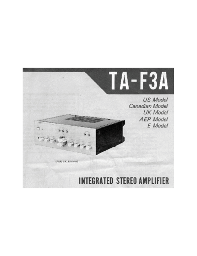
Service Manuals, User Guides, Schematic Diagrams or docs for : Sony SONY TA-F3A
<< Back | HomeMost service manuals and schematics are PDF files, so You will need Adobre Acrobat Reader to view : Acrobat Download Some of the files are DjVu format. Readers and resources available here : DjVu Resources
For the compressed files, most common are zip and rar. Please, extract files with Your favorite compression software ( WinZip, WinRAR ... ) before viewing. If a document has multiple parts, You should download all, before extracting.
Good luck. Repair on Your own risk. Make sure You know what You are doing.
Image preview - the first page of the document
>> Download SONY TA-F3A documenatation <<
Text preview - extract from the document
                                                           SPECIFICATIONS
GENERAL                                                                                Weight:    Approx.   10.5 kg (23 lb 2oz). net
                                                                                                  Approx.   12.5 kg (27 lb 9 oz), in shipping carton
   Power Requirements:   120V ac, 60 Hz (US, Canadian Model)                                                (US, Canadian Model)
                         220 V ac, 50160 Hz (AEP Model)                                           Approx.   9.5 kg (21 lb), net
                         240 V ac, 50/60 Hz (UK Model)                                                      11.5 kg (25Ib 6oz), in shipping carton
                         120 or 220V ac adjustable. 50/60 Hz (E Model)                                      (AEP, UK, E Model)
    Power Consumption:   85 W (US Model)
                         140W [Canadian Model)                       AMPLIFIER SECTION
                         210W (AEP, E Model)
                         240W (UK Model)                                        Continuous RMS
                                                                                  Power output:   Both channels driven simultaneously
           Dimensions:   Approx. 435 (w) x 145 (h) x 370 (d) mm           (Less than 0.5% THD)     At 1 kHz
                                    17 1/8(w) x 53/4(h) x 14%ldl inches                              5OW+5OW (8nl
                                   (US, Canadian Model)                                            At 20 Hz-20 kHz
                         Approx. 410 (w) x 145 (h) x 370 (d) mm                                      5OW+5OW(SI~l
                                   161/4(w) x 5%(h) x 141/,ldl inches                              According to DIN 45500 (AEP, UK, E Model)
                                    (AEP, UK, E Model)                                               52W+52W 03.Q)
                         Including projecting parts and controls
                                                                        Power Bandwidth (IHF):    10 Hz-25 kHz
          SAFETY-RELATED COMPONENT WARNING!!                                  Damping Factor:     30
     COMPONENTS IDENTIFIED BY SHADING AND A
                                                                         Harmonic Distortion:     Less than 0.5% at rated output
     MARK ON THE SCHEMATIC DIAGRAMS, EXPLODED                                                     Less than 0.1 % at 1 W output
     VIEWS AND IN THE PARTS LIST ARE CRITICAL TO
     SAFE OPERATION. REPLACE THESE COMPONENTS                                   IM Distortion:    Less than 0.5 % at rated output
     WITH SONY PARTS WHOSE PART NUMBERS APPEAR                            (60 Hz: 7 kHz = 4:1)    Less than 0.1% at 1W output
     A8 SHOWN IN THIS MANUAL OR IN SUPPLEMENTS
     PUBLISHED BY SONY.

          ATTENTION AU COMPOSANT AVANT RAPPORT
1-2. CIRCUIT DESCRIPTION                                       3. Muting Circuit (See Fig. 1-3 and Fig. 1-4)
                                                                   This muting circuit prevents the loud "pop" (due
PROTECTION CIRCUIT                                                 to initial current flow) or click noises produced
                                                                   just after turning the POWER switch to on or off.
   Two kinds of protection circuit are employed in                 These transients might damage a delicate high-
this power amplifier.    One is a power-transistor                 fidelity speaker system.
protection circuit and the other is a speaker pro-
tection circuit.                                               .   When POWER Switch turned on:
                                                                   C308 commerces to charge through R309. At the
1. Power-transistor Protection Circuit                             same time, the base voltage of Q306 gradually
  To protect overloaded power transistors from                     rises in accordance with charging voltage of C308.
  destruction, a protection circuit is employed. The               It takes about 3 seconds until Q306 is turned on.
  fusible resistors are inserted in each of Q704,                  Accordingly, the speaker output terminal is cut off
  4705 (L-CH) and 4754, 4755 (R-CH) collector                      by the relay RY301 for about 3 seconds after the
  and emitter circuits. When the excessive current                 POWER switch is turned on. This protects the
  flows into the power transistors, these fusible                  speaker from the destruction caused by the "pop"
  resistors break faster than the transistors and thus             noises.
  protects the transistors from destruction.
   Speaker Protection Circuit (See Fig. l-l and Fig. 1-2)
   When the excessive current flows into the power
   transistors, B+ voltage decreases. Therefore, 4301
   turns on, biasing the base of Q302, and Q302
   conducts. This removes the bias voltage at the
   base of Q306 and Q306 turns off. The relay is
   not activated by off state of Q306. According-
   ly, the speaker is cut off from the amplifier
   circuit.
   When the positive dc component presents at the
   speaker output terminal, C310 is charged up as
   shown in Fig. l-2. Q303 turns on, Q306 turns off
   and the relay RY301 is not activated (4304 re-                                    Fig. 1-2.
   mains in off condition). Also, when the negative
   dc component presents, C3 11 is charged up. This
   turns 9304 on, Q306 off and RY301 is not                    . When POWER Switch turned off:
   activated (9303 remains in off condition).
                                                                   The reverse voltage (about - 1.7 V) that turns off
                                                                   Q306 immediately reduces, and the positive poten-
                                                                   tial is applied to the base of Q305. Q305 turns on
                                                                   and Q306 turns off, cutting off the operation of
                                                                   RY301. Therefore, no pop noise presents on the
                                                                   speaker output.


                                                                                  POWER Switch :ON


                      Fig. l-1.                                                      Fig. 1-3.


                                                         -4-
◦ Jabse Service Manual Search 2024 ◦ Jabse Pravopis ◦ onTap.bg ◦ Other service manual resources online : Fixya ◦ eServiceinfo