Service Manuals, User Guides, Schematic Diagrams or docs for : Sony sony tv bulletins sony tv bulletins TVP0428
<< Back | HomeMost service manuals and schematics are PDF files, so You will need Adobre Acrobat Reader to view : Acrobat Download Some of the files are DjVu format. Readers and resources available here : DjVu Resources
For the compressed files, most common are zip and rar. Please, extract files with Your favorite compression software ( WinZip, WinRAR ... ) before viewing. If a document has multiple parts, You should download all, before extracting.
Good luck. Repair on Your own risk. Make sure You know what You are doing.
Image preview - the first page of the document
>> Download TVP0428 documenatation <<
Text preview - extract from the document
CONFIDENTIAL CSV-1
Sony Service Company
National Technical Services Service Bulletin
A Division of Sony Electronics Inc.
Park Ridge, New Jersey 07656 TV Products
Model: KV-32S40, KV-32S42, KV-32S45, KV-32S65 No. 428R2
KV-32S66, KV-32V40, KV-32V42, KV-35S40
KV-35S42, KV-35S45, KV-35S65, KV-35S66
KV-35V42
Subject: Black Pencil Line (Half Moon Shape Curve Date: July 20, 2000
Line) on left Side Of The Picture
Symptom:
(1334) With a dark scene a curved running top to bottom black pencil line appears on the left
side of the screen. This can occur in RF or Video Modes.
Solution: If the customer should complain about this symptom the line can be minimized by the
following circuit change.
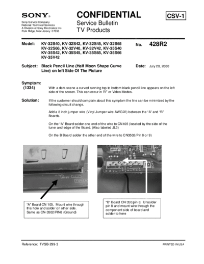
Add a 8 inch jumper wire (Vinyl Jumper wire AWG22) between the "A" and "B"
Boards.
On the "A" Board solder one end of the wire to CN105 (located by the side of the
tuner and edge of the Board. (Also labeled JL3)
On the B Board solder the other end of the wire to CN3502/Pin 8 or 9)
"B" Board CN 350/pin 8. Unsolder
"A" Board CN 105. Mount wire through pin 8 and mount wire through the
this hole and solder on other side. component side of board and
Same as CN-3502/PIN8 (Ground) solder to here
Reference: TVSB-299-3 PRINTED IN USA
◦ Jabse Service Manual Search 2024 ◦ Jabse Pravopis ◦ onTap.bg ◦ Other service manual resources online : Fixya ◦ eServiceinfo