Service Manuals, User Guides, Schematic Diagrams or docs for : Tektronix publikacje 1966SC
<< Back | HomeMost service manuals and schematics are PDF files, so You will need Adobre Acrobat Reader to view : Acrobat Download Some of the files are DjVu format. Readers and resources available here : DjVu Resources
For the compressed files, most common are zip and rar. Please, extract files with Your favorite compression software ( WinZip, WinRAR ... ) before viewing. If a document has multiple parts, You should download all, before extracting.
Good luck. Repair on Your own risk. Make sure You know what You are doing.
Image preview - the first page of the document
>> Download 1966SC documenatation <<
Text preview - extract from the document
/
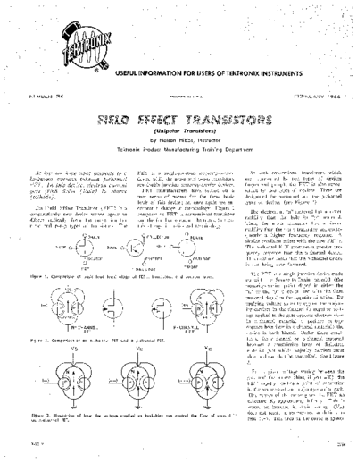
USEFUL INFORMATION FOR USERS OF TEKTRONIX INSTRUMENTS
NUMBER 3 6 PRINTED IN U.5.A FEBRUARY 1966
(Unipolar Transistors)
by Nelson Hibbs, Instructor
Tektronix Product Manufacturing Training Departmenf
At lasf w e have eulzat a ~ ~ l o z t t~ ~a s
o t F E T is a single-junction wbjority-cczrrir~ As with conventional tr;insistors, which
backward vacztu~il tube-a p-clza~zlrcl tlevice while the n-p-n and 1)-n-p transistors are represented by two types of devices
F E T . In tlzis device, electron cztrregzt a r e double-junction ~ili~~oriiy-carrier devices. (n-1)-n and p-n-p), tlie FET is also repre-
goes f r o m draitz (plate) t o sozr~cc F E T manufacturers have settled on a sented by two types of tlcvices. These a r e
(cathode). new series of names for the three basic designated tlie n-channel and the p-channel
leads of this device; so, once again we en- types of devices (see Figure 2 ) .
The Field Effect Transistor ( F E T ) is ;L counter a cl~angein terminology. Figure 1
T h e electron in "n" rnaterial has a faster
compar;itively new device whose operation compares an F E T , a convention;d transistor
differs radically from the more familiar mobility th:m the hole in "p" material.
and the familiar vacuum-tube triode to s h o ~ v
n-p-n and p-n-p types of transistors. T h e Thus, the n-p-n transistor has :i faster
this change in basic-lead terminology.
~iiol)ilityt11:~n the p-11-p transistor and conse-
quently a higher f requency response. A
similar condition exists with the new FET's.
T h e 11-channel F E T promises a greater fre-
quency response than the p-channel device.
FET
8 "ITTER
TRANSISTOR
CATHODE
TRIODE
This does not mean that the p-channel device
is not being tnanufactured.
T h e F E T is a single-junction tlevice made
Figure 1. Comparison of basic lead terminology of FET's, transistors, and vacuum tubes.
up with the Source-to-Drain material (the
majority-carrier path) doped in either the
"n" o r the "p" direction and with the Gate
material doped in tlie opposite direction. By
applying voltage s o a s to oppose the major-
ity carriers in the channel ( a negative volt-
age applied to the gate opposes electron flow
in n-channel material-a positive voltage
I N-CHANNEL
FET
I -CHANNEL
FET
opposes hole flow in p-channel material) the
device is back biased. Under these condi-
Figure 2. Comparison of an n-channel FET and a p-channel FET. tions, the n-channel o r p-c1i;unnel material
becon~es a constrictive layer of dielectric
VD vD "D material past \\.Iiich majority carriers must
flow : ~ n dcan thus be controlled. See Figure
3.
F o r a given vollage setting between the
gate :md the source (bias, if you will), the
F E T rapidly reaches a point of saturation
in the source-to-drain majority-carrier path.
This region of the curve gives the F E T an
effective R,, approaching infinity. This is
\vliere an increase in drain voltage (VD)
docs not result in an increase in drain cur-
Figure 3. Illustration of how the voltage applied as back-bias can control the flow of current in
an n-channel FET. rent ( I D ) . T h i s area of the curve is spoken
THE FET T R A
Figure 6. Comparison of an FET and a Unijunction transistor.
Operational g,, = g,,, ( a t zero bias) into the n material between the emitter and
r 3 base # 1 thus reducing the ohmic resistance
of the contact. T h e FET operates with a
voltage-driven gate and the resultant back-
biased junction with the field restricting the
Now, with a truly representative g,,, avail- majority-carrier flow through the body of
able, one can closely predict the voltage the device. Tlie F E T , like a vacuum tube,
gain of the tlevice in a circuit by using the is a nortnally "ON" device and n ~ u s t be
l'entotle A , formula : turned " O F F . Conversely, the unijunction
Figure 4. A chart of VD vs ID curves of on
.A, = operational g,,, x RI,. transistor is :I normally " O F F device (as a
FET showing the pinch off region and Ohmic
region at different values of bias voltage. result of the ohmic contacts) and must be
Noting that the input to the device is a turned "ON" by the signal a t the emitter-
bacli-biased diode, one can see that it offers two totally different theories of operation.
a high input impedance and that this haclc-
hinsed junction will show a capacitative T o summarize the properties and charae-
effect from gate-to-source and from source- teristics of tlie F E T :
to-drain. T h e latter also gives a miller A. Input Impedance :
effect. Note also, that the input-impedance
\\.ill decrease with increasing frequencies :it 1. T h e F E T is a high-input impedance
device, the input terminal is essen-
tially looking into a reverse-biased
which the product becomes compa-
'"fCcs junction.
sable to tlie input resistance. Also, the gain- 2. Tlle FET has input capacitance that
band\\itltli product will be approximatel) : varies inversely with VW (bias)
See Figure 7.
Gain Bandwidth B. Mode of operation
Again, s i ~ n i l a rto the vacuum tuhe pentode 1. T h e F E T is a voltage-co~itrolled
This dictates the usual coinpromise bet wee^^ tlevice just a s a vacuum tube pentode.
VD (VOLTS)
gain m 11:~ndwidth when using this tlevice.
d 2. T h e F E T has a very, very high R,,
Figure 5. A chart of the VI, vs In curves of Tlie F E T shoultl not lx confusetl with [lie (R,,) cli:~racteristic similar to a
another FET showing Zener-knee breakdown of \ - : ~ u u mtube pentode.
Gate-to-Drain back-biased diode. An exten- Vnijuiiction Transistor. Tlie tlieory of oper-
sion of the curves shown in Figure 4 would ation is totally different, ;dtIiough :\t first 3. T h e F E T has a consistently non-
reveal a similar tendency of this FET to ava- glance, tlie unijunction trat~sistor loolis ;\I- linear g,,, characteristic.
lanche at some certain VD voltage. most like an 11-c1i:mncl F E T . See Figure 6
for a comparison. C. Output 111ipctlance :
of as the "Pinch-Off Region". See Figure T h e unijunction transistor operates ns a 1. Tlie F E T is a high-output imped:mce
4. The area t o the side of this (where :ln current-driven tlevice with a forword-hic~scri tlevice (current source). However,
increase in VD results in an incl-e:w in junction of 1)-to-n m:~terial injecting holes cl~fferent means of manufacturing
ID-close to the graph a s i s ) is termed the
"Ohmic Region".
A study of the VD vs ID curves (see
Figure 5 ) shows that with a given load
line, the resultant transfer curve is non-
linear. This non-linearity is relative to tlie
deviation in the resistance represented in the
majority-carrier path a s controlled 11) the
biasing voltage. T h e best "g,,," occurs under
zero bias conditions and the forward voltage
at which saturation of this path occurs is
called V, (pinch-of f voltage). V, is counted
as a characteristic of the individual device.
Thus, in order t o find tlie active g,,, a t a
bias different than zero, w e must multiply
the zero-bias g,,, by the factor one minus Figure 8. Plot showing leakage current from
the ratio of gate voltage-to-pinch-ofi volt- -
Source - to - Gate (Isco) and Drain to - Gate
Figure 7. Variation of Source-to-Gate and (IDGO) against temperature under zero bias
age raised to the two-thirds power. Drain-to-Gate capacitance with voltage. conditions.
may result in relatively low ratings tection against thermal run away. This Sweep set to N P N (for 11-channel F E T ' s )
of t h i s characteristic in comparison statement is not wholly true in the case of or P N P ( f o r p-cha~~nel E T ' s ) . The
F
with t h e vacuum tube pentode. M O S (hfetal-Oxide-Insulatetf) FET's. P O L A R I T Y control of the Base Step
Generator should be set to M I N U S for n-
Another noteworthy characteristic of The M O S FET's separate the gate and channel and P L U S for p-channel FET's.
FET's is t h e i r built-in protection against channel with a layer of intrinsic material.
thermal run away. Because the input is a As temperature increases on this device, the F E T ' s that require more than 2.4 volts to
back- biased diode, the thermal - sensitive channel apparently increases also as it starts drive them to cut off-and the great major-
backward current (leakage current) flo\vs to include some of the insulating layer into ity are in this categorjr-will require that a
from both t h e source-to-gate ( 1 s ~ )and the main channel. The M O S F E T reacts 1 I&, 1% resistor be connected between
drain-to-gate (Inco). Plotting this linear more to changes in temperature than the the B A S E ( G A T E ) and E M I T T E R
current against temperature under zero bias regular FET's even though they do a\va> ( S O U R C E ) binding posts on the test panel
conditions of the other element gives two with leakage currents in the gate circuit. of the Type 575. This, in order to convert
straight line projections as shown in Figure the B A S E current, as indicated by the
\Vith standard FET's, leakage currents in
8. STEP S E L E C T O R switch in MA, to Gate
the gate lead have been reduced to the Vcs voltage in volts. Thus, 1 mA per
This increase in leakage current in the neighborhood of 0.001 to 0.0001 niA and step into 1 k a gives 1 volt/step and twelve
gate junction has a resistive effect on the this can be tolerated where instability of 11, steps at 1 tnA per step can give up to 12
majority-carrier path resulting in a lower with temperature change cannot. volts-ample in most instances to drive any
saturation current for a given bias voltage.
Characteristic curves of F E T ' s can be F E T to cut off.
For a g r a p h of this action under zero bias
conditions, and with the forward voltage displayed on a Type 575 Transistor-Curve The four waveforms represented in Fig-
froni the d r a i n to the source set at 50 volts, Tracer. The E M I T T E R - G R O U N D ures 10, 11, 12, and 13 were obtained in this
see Figure 9 ( a ) . A cross graph of g,,, and ( S O U R C E - G R O U N D ) mode is used with manner. The F E T used in these tests was
output resistance plotted against temperature the P O L A R I T Y control of the Collector an Amelco U-1346 field effect transistor.
is shown in Figure 9 ( b ) . The conlbination
tal) = 2 V/cm, ID (vertical) = 1 mA/cm. Figure 1 1 . Drain current vs Gate Source Volt-
age (ID vs Vcs with VDS constant). Vcs (hor-
izontal)= 0.5 V/cm, l ~ s s(vertical) = 1 mA/
cm.
Figure 9. ( a ) Graph of saturation current
under zero b i a s conditions and with the forward
voltage from Drain-to-Source set at 5 0 volts.
( b ) Cross g r a p h of g, and output resistance
plotted ogainst temperature.
of these t w o reactions to temperature is
Such that a s temperature goes up, g,e goes
down and R, (counterpart of R, in vacuum
tubes) goes up. In other words, as the gate
starts to lose control of the drain current, a
greater portion of the actual drain current (horizontal) = 0.5 vlcm, lnss (vertical) =
will be passed on to the load resistor thus 2 mA/cm. Center vertical graticule line is zero
tending to lllaintaill the s;lme of bias. .Negative bias to left, positive bias to Figure 13. Drain curves showing avalanche
right of center line. Crowding of markers on (breakover ot the Gote-to-Collector Zener
voltage at t h e output. This is what we mean Knee). Vcs (horizontal) =
5 V/cm, l ~ s s(ver-
right hand side is due to gate drawing cur-
when we s a y that F E T ' s have built-in pro- tical)= 0.5 rnA/cm.
T e n films produced by Tektronix, Inc. contained in square waves a r e harmonically electronic computer and comn~unication
h a v e been certified as education films by related. T h e film demonstrates the basic systems.
the U . S . Information Service. These films use of the square wave generator and oscil-
"Thevenin's Theorem" . . . A 12-minute
a r e available on free loan a s an aid to loscope antl resulting information obtained
hlack antl white sound film. Presents a
companies engaged in educational o r train- f r o m distortions. I t discusses risetime antl
simplified approach to solving a n electronic
ing programs f o r their employees; or, if its importance in testing nlodern high speed
circuit which would otherwise involve com-
preferred, the films may be purchased. electronic equipment. Suitable for audi-
plex mathematics.
ences with at least a basic knowledge of
Interested persons should contact their electrical theory. "Solving the Unbalanced Bridge . . . A
local Tektronix Field Office, Field Engi- 17-minute black and white sound film.
neer, Field Representative o r Distributor. "Transmission Lines" . . . A 23-minute Normally a solution to a n unbalanced bridge
blaclc and white sound filni. Discusses the problem requires considerable matlieinatics
Listed below a r e the film titles, along
iuntlamentals of transmission lines. Ani- involving three simultaneous equations. This
with a brief review of the film:
mated drawings illustrate how electrical lecture film shows and explains how simply
" T h e Oscilloscope D r a w s a Graph" . . . energy is transmitted along a line. A n this can be acco~nplished using Thevenin's
A 20-minute color film in sound. T h e film oscilloscope shows how reflections can oc- Tlieorp and Ohm's law.
cur in a line. Characteristic impedance, the
explains that the oscilloscope display is "Triode Plate Characteristics . . . A
usually in the f o r m of a graph, and dc- importance of proper terminations, line
16-minute black and white sound filtn. Dis-
scribes how to read o r interpret the dis- losses, time delay, and velocity factor a r e
cusses plate characteristics of a typical tri-
play. also discussed.
ode (6DJ8) showing how the three basic
tube characteristics, amplification factor,
" T h e Cathode-Ray Tube, Window to "Timc and Quantity" . . . A 27-minute
plate resistance, antl transconductance, may
Electronics" . . . A 35-minute color film blaclc antl white filni in sound. Discusses
be determined from a set of plate curves.
in sound with animated seouences. This the measurement of time and quantity from
I t also plots a load line and shows how to
film explains in simple terms how a cathode billions of years to billionths of a second.
determine the gain of a simple aniplifier
r a y tube worlis. I t depicts the heart of the Slio\vs the importance of the oscilloscope
from these curves. I n addition a continu-
oscilloscope, the cathode ray tube, a s it is as the basic means of making accurate
ous display of the curves of a tube under
used in radar, sonar and manv other elec- measurcnients of very small segments of
actual operating conditions is shown on the
tronic systems, including computers. T h e time.
Type 570 Characteristic Curve Tracer, a
film also sliows the step-by-step manufac- special-purpose Tektronix oscilloscope.
t u r i n g proceqs of cathode ray tubes at Teli- "The Oscilloscope, \\/hat I t Is-\\'hat It
tronix, from the forming of metal "gun" Does" . . . A nine-minute color sound film. "Ceramics and Electronics" . . . A 22-
parts t o the final testing of completed tubes. Presents a non-teclu~ical explanation of tlie minute color filni with sound. Shows the
oscilloscope antl its uses. Stresses tlie im- importance of ceramic elements in the
" T h e Square \\lave" . . . A 25-minute portance of the instrument a s a measuring electronic intlustries antl stresses the appli-
black and wliite sound filni. Discusses tlie tool in electronic ;ind other fields. Oscillo- cation of ceramic insulating strips and otlier
theory of square waves, employed in com- scopes measure physical data in relation ceramic parts in oscilloscopes. I t also shows
puters and many other electronic devices; to sm;dl :umounts of time. T h e y ;me used the complete manufacturing process, in-
usually, in the f o r m of coded information. in research, engineering, and education, and cluding mixing of clays, firing, and glaz-
Anin~a!etl drawings show how sine waves in production testing and maintenance of ing, at Tektronix.
I n the October, 1965 issue of Service "Current Measurements a t Nanosecond measurements at n;tnosecond speeds
Scope t ~ v o typographical errors involving Speeds" is the title of an article written
Author of the article is Murlan R. Kauf-
part numbers, slipped by your editor. Both by a Telitronix engineer and published in
e r r o r s occurrcd in the article "Type M the octoher, 1065 issue of ELECTRONIC man, Design Engineer with the Digital
Four-Trace Plug-In Unit-Channels A, R, DESIGN NE\VS, ~ 1 , ~ ( ~ the ~
i Instrument group a t Tektronix, Inc. ~
~ ~ ~ Re- ~ ~
C, and D : Crosstalk". T h e part number problems encountered when attelllptillg to prints of the article a r e available. Con-
listed as 283-0050-00 should have read 213- measure nanosecond and sub-nanosecond tact your local Tektronix Field Office,
000.3-00; ;end tlie part number listed as 210- current pulses. I t describes the use o f a Field Engineer, Field Representative o r
0001-00 sliould have read 210-0201-00. current transformer f o r accurate current Ilistributor.
CRT MESH FILTER AND RFI DUST COVERS FOR OSCILLO- TEST POINTS FOR B PLUS
SCOPES
Tektronix engineers have come up with
a new C R T light filter and R F I shield
that is unique. This new C R T Mesh Light
Filter and R F I Shield is a metal screen
of sub-visible mesh with the surface treated
for extremely low reflectance. T h e screen
is tautly mounted on a metal frame. This
unique filter-shield is a direct replacement
for the e x i s t i n g graticule cover on most
Tektronix oscilloscopes. T w o exceptions
are the T y p e 422 and Type 453 Portable
Oscilloscopes. The filter-shield f o r these
Figure 2. Short pieces of bare wire installed
instruments snaps into the C R T opening os B-plus test points in the ceramic strips of
on the f r o n t panel. o Type 5 4 5 8 Oscilloscope.
The purpose of this new mesh filter-shield
is to enhance visual C R T trace-to-bacli- I,. I?. Risllel, with the Otis Air Force
ground contrast and attenuate R F I radi- Base in M:~ssacllusetts, has submitted to
ated from t h e C R T faceplate. I t accom- the Air Force :tnd to Service Scope, a
plishes these purposes very well intleed. Figure 1. New dust cover for Tektronix oscil- "do-it-yourself" modification that you may
The curtailment of external atnhient ligllt loscopes shown on a Type 545B Oscilloscope. want t o adopt.
reflections is highly efficient. Trace-to- T h e suggestion involves installing short
b:tcl
◦ Jabse Service Manual Search 2024 ◦ Jabse Pravopis ◦ onTap.bg ◦ Other service manual resources online : Fixya ◦ eServiceinfo