Service Manuals, User Guides, Schematic Diagrams or docs for : acer Acer Aspire 7110 9410 9420 - WISTRON MYALL2 - REV MPSec

<< Back | Home

Most service manuals and schematics are PDF files, so You will need Adobre Acrobat Reader to view : Acrobat Download Some of the files are DjVu format. Readers and resources available here : DjVu Resources
For the compressed files, most common are zip and rar. Please, extract files with Your favorite compression software ( WinZip, WinRAR ... ) before viewing. If a document has multiple parts, You should download all, before extracting.
Good luck. Repair on Your own risk. Make sure You know what You are doing.


Image preview - the first page of the document
Acer Aspire 7110 9410 9420 - WISTRON MYALL2 - REV MPSec


>> Download Acer Aspire 7110 9410 9420 - WISTRON MYALL2 - REV MPSec documenatation <<

Text preview - extract from the document
                        A                                                      B                                                 C                                                      D                                                 E


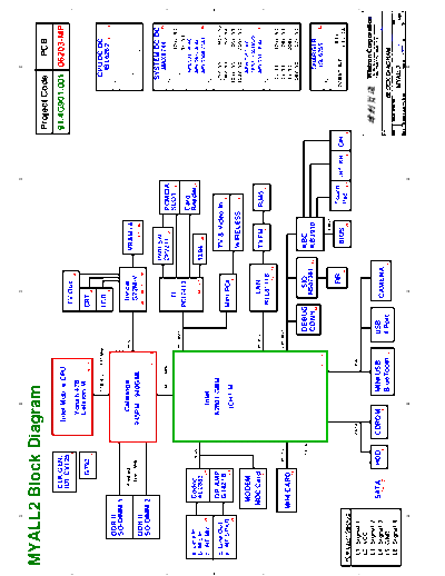
    MYALL2 Block Diagram                                                                                                                                                                            Project Code                                  PCB
                                       CLK GEN.                         Intel Mobile CPU                                                                                                            91.4G901.001 06203-MP
                                       IDT CV125                                                                           TV Out
4                                                       3                                                                                                                                                                                                                            4
                                                                                                                                          14
                                                                         Yonah 478
                                                G792                     Celeron M                                         CRT
                                                                                           4~5
                                                       19                                                                       14

                                                                                   FSB 400/533/667 MHz
                                                                                                                           LCD                                                                                                     CPU DC/DC
                                                                                                                                13                                                                                                  ISL6262 37 ~ 38
             DDR II                                                                                                                                                                                                              INPUTS             OUTPUTS
             SO-DIMM 1
                            11 ~ 12      RAM BUS                       Calistoga                          PEG               Nvidia                                                                                                       VCC_CORE
                                                                                                                                                        VRAMx4                                                                  DCBATOUT 0.844~1.3V
                                         533/667 MHz
                                                                    945PM / 940GML                                          G72M-V                            49 ~ 50                                                                     27A
             DDR II                                                                                                        46 ~ 48 , 51 ~ 55
             SO-DIMM 2
                                                                                                 6 ~ 10
                            11 ~ 12
                                                                                                                                                      PWR SW                                                                      SYSTEM DC/DC
                                                                                                                                                                                                                                        MAX8744                       35
                                                                                   DMI 100 MHz                                                        CP2211 25
3
                                                                                                                                                                            PCMCIA                                               INPUTS             OUTPUTS
                                                                                                                                                                                                                                                                                     3


                                                                                                                             TI                                             SLOT 27                                                                    3D3V_S5
                                                                                                          PCI BUS                                                                                                               DCBATOUT
                                                                                                                           PCI7412                                                                                                                     5V_S5
                                                                                                                                                                            Card                                                    APL5331-KAC
      a. Line In                  Codec                HDA                                                                                                                  Reader26                                                APL5912-KAC
      b. Mic In                   ALC883                                                                                        24 ~ 25
                                                                                                                                                      1394   26                                                                     APL5308-25AC 40
      c. INT Mic   29                           28
                                                                            Intel                                                                                                                                                INPUTS   OUTPUTS

      d. Line Out                 OP AMP                                 82801 GBM                                                                       TV & Video-In                                                           1D5V_S5               1D05V_S0
      e. INT.SPKR                 G1421B                                                                                   Mini-PCI                                           30                                                 1D8V_S3               1D5V_S0
                                                29
                   29                                                      ICH7-M                                                      30                                                                                        3D3V_S5               1D5V_S5
                                                                                                                                                         WIRELESS             30                                                 3D3V_S0               2D5V_S0
                                MODEM                                                                                                                                                                                               APW7057-KC
                                                                                                                                                                                                                                    TPS51100DGQ
                               MDC Card                                                                   PCIE x 1              LAN                      TXFM               RJ45                                                    APL5331-KAC 41
2                                               21                                                                                                                                                                                                                                   2

                                                                                                                           RTL8111B                               23               23                                            INPUTS   OUTPUTS
                                                                                                                                       22 ~ 23
                                                                                                                                                                                                                                  5V_S5                3D3V_S5
                                                     PCIE x 1                                             LPC BUS                                                                                                                 5V_S5                1D8V_S3
                             MINI CARD                                                                                                                                                                                            5V_S5                0D9V
                                                26
                                                                                                                                                                                                                                 1D8V_S0               1D2V_S0
                                                        SATA                                                     DEBUG               SIO                 KBC
                                                                                                                 CONN34         NS87381           32     KB3910                                                                         CHARGER
                                                                                                                                                                       31                                                                ISL6255                      42
                                                                                             15 ~ 18
                                                                                                                                                                  X BUS
                                                                                                                                                                                                                                 INPUTS             OUTPUTS

                                                                                                                                     FIR                                     Touch                                                                        BT+
                                                                                                                                                             BIOS                   INT. KB CIR                                 DCBATOUT
                                                                                                                                            32                                                                                                         16.8V 3A
    PCB Layer Stackup                                                                                                                                              34        Pad 33       33   33

1     L1: Signal 1                                               PATA                        USB                                                                                                                                                                                     1


      L2: VCC
                                                                                                                                                                                                                                  Wistron Corporation


                                                                                                                                                                                                                                                                                om
      L3: Signal 2                                                                                                                                                                                                                21F, 88, Sec.1, Hsin Tai Wu Rd., Hsichih,


                                                                                                                                                                                                                                                                           l.c
                                  SATA               HDD         CDROM             MINI USB                     USB                                                                                                               Taipei Hsien 221, Taiwan, R.O.C.


                                                                                                                                                                                                                                                                       ai
      L4: Signal 3                                                                                                            CAMERA


                                                                                                                                                                                                                                                                    tm
                                      24 ~ 25               20            20                                                                                                                    Title
                                                                                   BlueTooth                    4 Port21


                                                                                                                                                                                                                                                                  ho
      L5: GND                                                                                                                                    13
                                                                                                     21                                                                                                                  BLOCK DIAGRAM


                                                                                                                                                                                                                                                             f@
      L6: Signal 4                                                                                                                                                                              Size     Document Number                                                   Rev


                                                                                                                                                                                                                                                            in
                                                                                                                                                                                                                                MYALL2


                                                                                                                                                                                                                                                        xa
                                                                                                                                                                                                                                                                                MP


                                                                                                                                                                                                                                                       he
                                                                                                                                                                                                Date: Tuesday, April 11, 2006            Sheet     1         of            57
                        A                                                      B                                                 C                                                      D                                                 E
                            A                                                B                                               C                                             D                                                           E
    ICH7M Integrated Pull-up                                                                   954305D 27Mhz/LCDCLK Spread                                        Calistoga Strapping Signals and
    and Pull-down Resistors                             ICH7-M EDS 17837         1.5V1
                                                                                               and Frequency Selection Table                                      Configuration       EDS 17050 0.71
                                                                                                                                                                                                     page 7
                                                                                               SS3     SS2    SS1     SS0
                                                                                               Byte9   bit6   bit5    bit4       Spread Amount%          page 3    Pin Name      Strap Description                      Configuration
    EE_DIN, EE_DOUT, GNT[3:0], GPIO[25],                                                       bit 7                                                               CFG[2:0]     FSB Frequency Select
    GNT[4]#/GPIO48, GNT[5]#/GPO17, PME#,                                                        0      0      0       0           -0.50 Down                                                                     001 = FSB533
                                              ICH7 internal 20K pull-ups                                                                                                                                         011 = FSB667
    LAD[3:0]#/FHW[3:0]#, LAN_RXD[2:0]                                                           0      0      0       1           -1.00 Down                                                                     others = Reserved

4   LDRQ[0], LDRQ[1]/GPIO[41],                                                                  0      0      1       0           -1.50 Down                       CFG[4:3]     Reserved                                                                                         4
    PWRBTN#, TP[3]                                                                              0      0      1       1           -2.00 Down                       CFG5         DMI x2 Select                    0 = DMI x2
                                                                                                                                                                                                                 1 = DMI x4    (Default)
                                                                                                0      1      0       0           -0.75 Down                       CFG6         Reserved
    DD[7], DDREQ                              ICH7 internal 11.5K pull-downs
                                                                                                0      1      0       1           -1.25 Down                       CFG7                                          0 = Reserved
                                                                                                                                                                                CPU Strap                        1 =Mobile CPU(Default)
    ACZ_BIT_CLK, ACZ_RST#, ACZ_SDIN[2:0],     ICH7 internal 20K pull-downs                      0      1      1       0           -1.75 Down
                                                                                                                                                                                Reserved
    ACZ_SDOUT, ACZ_SYNC, DPRSLPVR/GPIO16,                                                       0      1      1       1           -2.25 Down                       CFG8
    EE_CS,SPI_ARB, SPI_CLK, SPKR,                                                               1      0      0       0           +-0.25 Center                                                                  0 = Reverse Lanes,15->0,14->1 ect..
                                                                                                                                                                   CFG9         PCI Express Graphics             1= Normal operation(Default):Lane
                                                                                                1      0      0       1           +-0.5 Center                                  Lane Reversal                         Numbered in order
    USB[7:0][P,N]                             ICH7 internal 15K pull-downs
                                                                                                1      0      1       0           +-0.75 Center
                                                                                                                                                                   CFG[11:10]    Reserved
    SATALED#                                  ICH7 internal 15K pull-up                         1      0      1       1           +-1.0 Center
                                                                                                                                                                                XOR/ALL Z test                   00 = Reserved
                                                                                                1      1      0       0           +-0.25 Center                    CFG[13:12]   straps                           01 = XOR mode enabled
    LAN_CLK                                   ICH7 internal 100K pull-down                                                                                                                                       10 = All Z mode enabled
                                                                                                1      1      0       1           +-0.5 Center                                                                   11 = Normal Operation
                                                                                                                                                                                                                 (Default)
                                                                                                1      1      1       0           +-0.75 Center
                                                                                                                                                                   CFG[15:14]   Reserved                           Reserved
    ICH7M IDE Integrated Series                                                                 1      1      1       1           +-1.0 Center
                                                                                                                                                                   CFG16        FSB Dynamic ODT                  0 = Dynamic ODT Disabled

3   Termination Resistors                                                                                                                                                       Global R-comp Disable
                                                                                                                                                                                                                 1 = Dynamic ODT Enabled (Default)
                                                                                                                                                                                                                 0 = All R-comp Disable                                          3
                                                                                                                                                                   CFG17        (All R-comps)                    1 = Normal Operation (Default)
    DD[15:0], DIOW#, DIOR#, DREQ,
                                              approximately 33 ohm
                                                                                               PCI Routing                              page 16
                                                                                                                                                                   CFG18        VCC Select                       0 = 1.05V (Default)
    DDACK#,    IORDY, DA[2:0], DCS1#,                                                                                                                                                                            1 = 1.5V
    DCS3#, IDEIRQ
                                                                                                                  IDSEL      INT -> PIRQ          REQ/GNT          CFG19        DMI Lane Reversal                0 = Normal operation (Default):lane
                                                                                                                             A->G, B->B,                                                                             Numbered in order
                                                                                                                                                                                                                 1 =Reverse Lane,4->0,3->1 ect...
                                                                                                7412                 22      C->F, D->G              0
                                                                                                                               A/C -> E                                                                          0 = Only SDVO or PCIE x1 is
    ICH7M Functional Strap Definitions                                             page 16
                                                                                                MiniPCI              21        B/D -> E              1             CFG20         SDVO/PCIE
                                                                                                                                                                                 Concurrent
                                                                                                                                                                                                                     operational (Default)
                                                                                                                                                                                                                 1 =SDVO and PCIE x1 are operating
                                                                                                                                                                                                                    simultaneously via the PEG port
     Signal          Usage/When Sampled                         Comment
                                                                                                                                                                   SDVOCRTL      SDVO Present                    0 = No SDVO Card present
    ACZ_SDOUT    XOR Chain Entrance/       Allows entrance to XOR Chain testing when TP3                                                                           _DATA                                             (Default)
                 PCIE Port Config bit1,    pulled low.When TP3 not pulled low at rising edge                                                                                                                     1= SDVO Card present
                 Rising Edge of PWROK      of PWROK,sets bit1 of RPC.PC(Config Registers:
                                           offset 224h)                                                                                                           NOTE: All strap signals are sampled with respect to the leading
                                                                                                                                                                        edge of the Calistoga GMCH PWORK in signal.
    ACZ_SYNC     PCIE bit0,                Sets bit0 of RPC.PC(Config Registers:Offset 224h)
                 Rising Edge of PWROK.
    EE_CS        Reserved                  This signal should not be pull high.
    EE_DOUT      Reserved                  This signal should not be pull low.
2   GNT2#        Reserved                  This signal should not be pull low.                                                                                                                                                                                                   2
                 Top-Block                 Sampled low:Top-Block Swap mode(inverts A16 for
    GNT3#        Swap Override.            all cycles targeting FWH BIOS space).
                 Rising Edge of PWROK.     Note: Software will not be able to clear the
                                           Top-Swap bit until the system is rebooted
                                           without GNT3# being pulled down.


    GNT5#/       Boot BIOS Destination     Controllable via Boot BIOS Destination bit
    GPIO17#,     Selection.                (Config Registers:Offset 3410h:bit 11:10).
    GNT4#/       Rising Edge of PWROK.     GNT5# is MSB, 01-SPI, 10-PCI, 11-LPC.
    GPIO48

    DPRSLPVR     Reserved                  This signal should not be pull high.
    GPIO25       Reserved.
                 Rising Edge of RSMRST#.   This signal should not be pull low.
    INTVRMEN     Integrated VccSus1_05     Enables integrated VccSus1_05 VRM when
                 VRM Enable/Disable.       sampled high
                 Always sampled.
    LINKALERT#   Reserved                  Requires an external pull-up resistor.
    REQ[4:1]#    XOR Chain Selection.
                 Rising Edge of PWROK.     TBD, Chapter 8.
1                                                                                                                                                                                                                                                                                1
    SATALED#     Reserved                  This signal should not be pull low.
    SPKR         No Reboot.                If sampled high, the system is strapped to the                                                                                                                                      Wistron Corporation
                 Rising Edge of PWROK.     "No Reboot" mode(ICH7 will disable the TCO Timer                                                                                                                                    21F, 88, Sec.1, Hsin Tai Wu Rd., Hsichih,
                                                                                                                                                                                                                               Taipei Hsien 221, Taiwan, R.O.C.
                                           system reboot feature). The status is readable
                                           via the NO REBOOT bit.                                                                                                                            Title

    TP3          XOR Chain Entrance.       This signal should not be pull low unless using
                                                                                                                                                                                                                            Reference
                 Rising Edge of PWROK.     XOR Chain testing.                                                                                                                                Size     Document Number                                                 Rev
                                                                                                                                                                                                                            MYALL2                                          MP
                                                                                                                                                                                             Date: Friday, March 24, 2006             Sheet     2         of          57
                             A                                                                           B                                                                           C                                                                          D                                                                           E


                                                                                                                                                                                                                                                                                                                                                   3D3V_S0
                             3D3V_S0    R448                                                                        R204                                                                                                                                                                                                         R437
                                        0R0603-PAD                                                                  0R0603-PAD                                                                                                                                                                                                   0R0603-PAD
                                        1        2 3D3V_CLKPLL_S0                                     3D3V_S0       1        2    3D3V_48MPWR_S0                                                                                                                                                        3D3V_CLKGEN_S0           2        1


                                 1


                                                                         1


                                                                                                                                                     1


                                                                                                                                                                                1


                                                                                                                                                                                                       1


                                                                                                                                                                                                                               1


                                                                                                                                                                                                                                                     1


                                                                                                                                                                                                                                                                           1


                                                                                                                                                                                                                                                                                                    1


                                                                                                                                                                                                                                                                                                                            1


                                                                                                                                                                                                                                                                                                                                                       1
                                     C647                                     C652                                                                        C626                      C633                    C636                   C655                  C654                  C653                     C637                    C625                         C632
                                                                              SC1U6D3V2ZY-GP                                                              SC1U6D3V2ZY-GP
                                     SCD1U16V2ZY-2GP                                                                                                                                SC4D7U10V5ZY-3GP        SCD1U16V2ZY-2GP        SCD1U16V2ZY-2GP       SCD1U16V2ZY-2GP       SCD1U16V2ZY-2GP          SCD1U16V2ZY-2GP         SCD1U16V2ZY-2GP              SCD1U16V2ZY-2GP


                                 2


                                                                         2


                                                                                                                                                     2


                                                                                                                                                                                2


                                                                                                                                                                                                       2


                                                                                                                                                                                                                               2


                                                                                                                                                                                                                                                     2


                                                                                                                                                                                                                                                                           2


                                                                                                                                                                                                                                                                                                    2


                                                                                                                                                                                                                                                                                                                            2


                                                                                                                                                                                                                                                                                                                                                       2
4                                                                                                                                                                                                                                                                                                                                                                                          4


     3D3V_S0
          1


              R426
              10KR2J-3-GP

                                                                                                                                                                                                                                                DREFSSCLK_1          4                1 RN67                          DREFSSCLK 7
          2


                                                                                                                                                                                                                                                DREFSSCLK#_1         3                2 SRN33J-5-GP-U                 DREFSSCLK# 7
                SS_SEL
                H/L: 100/96MHz                                                                                                                                                                                                                  CLK_MCH_3GPLL_1 4                     1 RN68                          CLK_MCH_3GPLL 7
          1


                                                                                                                                                               U41                                                                              CLK_MCH_3GPLL_1# 3                    2 SRN33J-5-GP-U                 CLK_MCH_3GPLL# 7
              R427 DY
              10KR2J-3-GP                                       31 PCLK_KBC                           R451
                                                                                                         2            1 33R2J-2-GP         PCLKCLK0       56                                                17     DREFSSCLK_1                  CLK_PCIE_ICH_1       3                2 RN73                          CLK_PCIE_ICH 16
                                                                                                                                                               PCI0                                LVDS            DREFSSCLK#_1                 CLK_PCIE_ICH_1#
                                                                                                                                                           3   PCI1                               LVDS#     18                                                       4                1 SRN33J-5-GP-U                 CLK_PCIE_ICH# 16
                                                                25       PCLK_PCM                     R441
                                                                                                         2            1   22R2J-2-GP       PCLKCLK2        4
          2


                                                                                                      R432                33R2J-2-GP       PCLKCLK3            PCI2                                                CLK_MCH_3GPLL_1              CLK_PCIE_LAN_1
                                                                32       PCLK_SIO                        2            1                                    5   PCI3                                SRC1     19                                                       3                2 RN71                          CLK_PCIE_LAN 22
                                                                34       PCLK_FWH                     R438
                                                                                                         2            1   22R2J-2-GP                                                                        20     CLK_MCH_3GPLL_1#             CLK_PCIE_LAN_1#      4                1 SRN33J-5-GP-U                 CLK_PCIE_LAN# 22
                                                                                                      R434                33R2J-2-GP       SS_SEL                                                 SRC1#            CLK_PCIE_ICH_1
                                                                30       PCLK_MINI                       2            1                                    9   PCIF1/SEL100/96#                    SRC2     22
                                                                16       CLK_ICHPCI                   R205
                                                                                                         2            1   33R2J-2-GP       ITP_EN          8                                                23     CLK_PCIE_ICH_1#              CLK_PCIE_SATA_1      4                1 RN69                          CLK_PCIE_SATA 15
                                                                                                      R433                10KR2J-3-GP                          PCIF0/ITP_EN                       SRC2#            CLK_PCIE_LAN_1               CLK_PCIE_SATA_1#
                                                                                                         2            1                                                                            SRC3     24                                                       3                2 SRN33J-5-GP-U                 CLK_PCIE_SATA# 15
                                                               16 PM_STPPCI#                                                                              55                                                25     CLK_PCIE_LAN_1#
                                                                                                                                                               PCI_STOP#                          SRC3#            CLK_PCIE_SATA_1
                                                                                                                 H/L : CPU_ITP/SRC7                                                                SRC4     26
                                                                                                                                                                                                            27     CLK_PCIE_SATA_1#
                                                                                                                                                                                                  SRC4#
                            PCLK_FWH & PCLK_PCM                 11,18 SMBC_ICH                                                                            46   SCL                                 SRC5     31
3                                                                                                                                                         47                                                30                                  CLK_PCIE_MINI_12     3                2 RN78                          CLK_PCIE_MINI2 26
                                                                                                                                                                                                                                                                                                                                                                                           3
                            need equal length                    11,18 SMBD_ICH                                                                                SDA                                SRC5#
                                                                                                                                                                                                            33     CLK_PCIE_MINI_12             CLK_PCIE_MINI_12#    4                1 SRN33J-5-GP-U                 CLK_PCIE_MINI2# 26
                                                                                                         RN66 SRN33J-5-GP-U                                                                        SRC6            CLK_PCIE_MINI_12#
                                                                                                                                                                                                  SRC6#     32
                                                                7         DREFCLK                        1         4                    DREFCLK_1         14                                                                                    CLK_PCIE_PEG_1       3                2 RN77 G72                      CLK_PCIE_PEG 46
                                                                                                                                        DREFCLK#_1             DOT96                                               CLK_PCIE_PEG_1               CLK_PCIE_PEG_1#
                                                                7        DREFCLK#                        2         3                                      15   DOT96#                      CPU2_ITP/SRC7    36                                                       4                1 SRN33J-5-GP-U                 CLK_PCIE_PEG# 46           When use UMA RN9 DUMMY
                         C648                                                                                                                                                                               35     CLK_PCIE_PEG_1#
                     SC27P50V2JN-2-GP                                                                                                                                                    CPU2_ITP#/SRC7#                                        CLK_CPU_BCLK_1       3                2 RN75                          CLK_CPU_BCLK 4
                        1     2                                  GEN_XTAL_IN                                                                              50                                                44     CLK_CPU_BCLK_1               CLK_CPU_BCLK_1#      4                1 SRN33J-5-GP-U                 CLK_CPU_BCLK# 4
                                                                 GEN_XTAL_OUT_R                   R444 2                                                       XTAL_IN                             CPU0
                                                                                                                      1 0R0603-PAD      GEN_XTAL_OUT      49   XTAL_OUT                           CPU0#     43     CLK_CPU_BCLK_1#
                                            1


                                                X4                                                                                                                                                          41     CLK_MCH_BCLK_1               CLK_MCH_BCLK_1       3                2 RN76                          CLK_MCH_BCLK 6
                                                X-14D31818M-31GP 32                                   R452                                                                                         CPU1
                                                                       CLK14_SIO                         2            1 22R2J-2-GP                                                                CPU1#     40     CLK_MCH_BCLK_1#              CLK_MCH_BCLK_1#      4                1 SRN33J-5-GP-U                 CLK_MCH_BCLK# 6
                         C640                   82.30005.831        16 CLK_ICH14                      R453
                                                                                                         2            1 22R2J-2-GP       GEN_REF          52
                     SC27P50V2JN-2-GP                                                                 R450                                                     REF
                                                                                                         2            1 475R2F-L1-GP     GEN_IREF         39                                                54                                                                                                        PM_STPCPU# 16
                                            2


                                                                                                                                                               IREF                          CPU_STOP#             CPU_SEL2
                        1     2                                                                                                                                                            FSC/TEST_SEL     53                                                                                                        CPU_SEL2 4,7
                                                                                                                                                                                                            16     CPU_SEL1                                                                                           CPU_SEL1 4,7
                                                                                                                                                                                         FSB/TEST_MODE             CLK48                         R436 22R2J-2-GP 2
                                                                    37        CLK_EN#                                                                     10   VTT_PWRGD#/PD                  USB48/FSA     12                                                                    1                                   CLK48_ICH 16
                                                                                                                 R435                                                                                                                            R428 22R2J-2-GP 2                1                                   CLK48_CARDBUS         25
                                                                                                                 10KR2J-3-GP                                                                                                                     R429 2K2R2J-2-GP 2               1          CPU_SEL0                 CPU_SEL0 4,7
                                                                                               3D3V_S0       2          1                                  2                                                34        3D3V_CLKGEN_S0
                                                                                                                                                               VSS_PCI                         VDD_SRC
                                                                                                                                                           6   VSS_PCI                         VDD_SRC      21

                                                                                                                                                          51   VSS_REF                          VDD_PCI     7
                                                                                                                                                          45   VSS_CPU                          VDD_PCI     1
                                                                                                                                                          38   VSSA
                                                                                                                                                          13   VSS48                           VDD_REF      48                                                                                                            FSC      FSB           FSA         CPU         FSB
                                                                                                                                                          29   VSS_SRC                         VDD_CPU      42
                                                                                                                                                                                                            37        3D3V_CLKPLL_S0                                                                                        0          0           0         266M        X
                                                                                                                                                                                                  VDDA                3D3V_48MPWR_S0                                                                                        0          0           1         133M        533M
                                                                                                                                                                                                 VDD48      11
                                                                                                                                                                                                            28                                                                                                              0          1           0         200M        X
2                                                                                                                                                                                              VDD_SRC                                                                                                                      0          1           1         166M        667M              2
                                                                                                                                                                                                                                                                                                                            1          0           0         333M        X
                                                                                                                                                               IDTCV125PAG-GP                71.00125.A0W                                                                                                                   1          0           1         100M        X
                                                                                                                                                                                                                                                                                                                            1          1           0         400M        X
                                                                                                                                                                                                                                                                                                                            1          1           1       Reserved      X
                                                                                                      RN63
                                                                                                      SRN49D9F-GP
                                                                              DREFSSCLK#          1            4                                                                                                                                                                                                      1D05V_S0
                                                                              DREFSSCLK           2            3


                                                                                                                                                                                                                                                                                         2


                                                                                                                                                                                                                                                                                                                        2


                                                                                                                                                                                                                                                                                                                                                             2
                                                                                                      RN62
                                                                                                      SRN49D9F-GP                                                                                                                                                                               R573 DY                     R574 DY                              R575 DY
                                                                              DREFCLK#            1            4                                                                                                                                                                                1K74R2F-GP                  1K74R2F-GP                           1K74R2F-GP
                                                                              DREFCLK             2            3


                                                                                                                                                                                                                                                                                         1


                                                                                                                                                                                                                                                                                                                        1


                                                                                                                                                                                                                                                                                                                                                             1
                                                                                                                                                                                                                                                                         CPU_SEL0                         CPU_SEL1                         CPU_SEL2


◦ Jabse Service Manual Search 2024 ◦ Jabse PravopisonTap.bg ◦ Other service manual resources online : FixyaeServiceinfo