Service Manuals, User Guides, Schematic Diagrams or docs for : acer Acer Aspire One Happy2 DA0ZE6MB6E0 QUANTA_ZE6-REV1B
<< Back | HomeMost service manuals and schematics are PDF files, so You will need Adobre Acrobat Reader to view : Acrobat Download Some of the files are DjVu format. Readers and resources available here : DjVu Resources
For the compressed files, most common are zip and rar. Please, extract files with Your favorite compression software ( WinZip, WinRAR ... ) before viewing. If a document has multiple parts, You should download all, before extracting.
Good luck. Repair on Your own risk. Make sure You know what You are doing.
Image preview - the first page of the document
>> Download Acer Aspire One Happy2 DA0ZE6MB6E0 QUANTA_ZE6-REV1B documenatation <<
Text preview - extract from the document
1 2 3 4 5 6 7 8
01
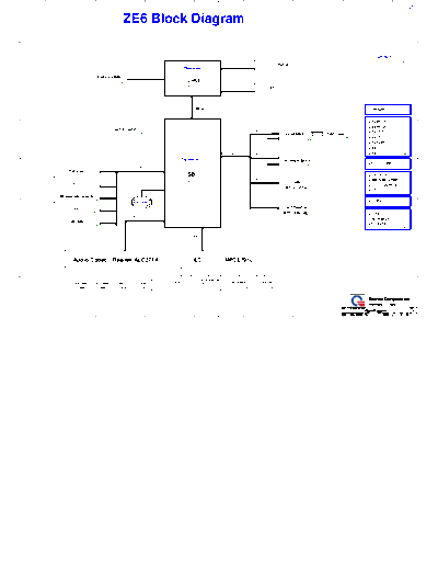
ZE6 Block Diagram
A A
CK505
P2
INT_LVDS 10.1 "Panel
DDR SYSTEM MEMORY
Pineview Up to 1280*800 or 1366*768
Graphics Interfaces
P14
DDRIII-SODIMM 667 MT/s
P3
CPU
P4,5,6,7 CRT CRT
DMI
P14
N570 1.66G: AJSLBXEVT05
N475 1.83G: AJSLBX5UT08
N455 1.66G: AJSLBX9VT05
DMI(x2) Charger
P27
B B
+3VPCU
SATA 0 DMI +5VPCU
SATA - HDD SATA PCIE-4
P19 SIM Card +3V_S5
USB-5 3G/WiMAX
P20 USB-4
P20 +5V_S5
+3VSUS
+3V
PCI-Express(Port1~4) PCIE-2 +5V P28
Tigerpoint
USB-7 WLAN/WiMAX
P20 VCC_CORE
USB 2.0 (Port0~7) P29
USB-0,1,3
USB port*3 USB PCI-E
P17 SB +1.5VSUS
PCIE-1
USB-2 P8,9,10,11,12,13 LAN +SMDDR_VREF
CCD +0.75V_DDR_VTT
P14 RTL8105TA
RTC P18 +1.5V P30
USB-6
C
Bluetooth module C
P15 PN : AJSLGXX0T14
BATTERY +1.05V
PCIE-3 P31
USB-5 Card Reader
3G P11
P20 RTS5209-GR
P21 +1.5V
Intel High Definition Audio
USB-7
IHDA
Discharge
WLAN
P20 LPC VCCGFX
P32
LPC
Audio Codec Realtek ALC271X EC NPCE791L
P16 P22
D D
Touch Pad /B
K/B Con. SPI Flash Charger
Int. SPK Int. AMIC MIC Combo Con.
CONN CONN Jack Jack P15 P15 P22 P24
Quanta Computer Inc.
PROJECT : ZE6
Size Document Number Rev
Block Diagram 1B
Date: Friday, March 11, 2011 Sheet 1 of 35
1 2 3 4 5 6 7 8
5 4 3 2 1
CLK GEN (CLK) 02
VDD_CLK_3.3V VDD_CLK_1.5V +1.5V
+3V R212 2.2/J_6
1 2 L22 +3V
PBY160808T-301Y-N/2A/300ohm_6
L20
PBY160808T-301Y-N/2A/300ohm_6 C191 C146 C195 PM_STPPCI#_R R163 10K/J_4
D <20100819_FAE Poyueh> Add 2.2ohm resistor for noise suppress D
Place close to L8 .1U/10V_4 .1U/10V_4 4.7U/10V/8
C188 C157 C163 PM_STPCPU# R153 10K/J_4
Place close to L13
C185 .1U/10V_4 .1U/10V_4 .1U/10V_4
0.1uF near every power pin CLKREQ_MPC#_R R149 10K/J_4
4.7U/10V/8
CLKREQ_MNC#_R R202 10K/J_4
U9
0.1uF near every power pin
CLKREQ_LAN#_R R148 10K/J_4
5 23 1/19 : 439549_439549_CorbettPark_Schm_Rev0.5: If this pin is
VDD_REF_3.3 VDD_CORE_1.5 used as PCI_STOP#, it is required to provide a 10-k pull-up to
9 45 Vcc3_3. It is not recommended to connect this signal to the USB_48M R374 20K/F_4
VDD_IO can be ranging VDD_PCI_3.3 VDD_CORE_1.5 Tiger Point(NM10) as it may cause unexpected system behavior.
from 1.05V to 3.3V. 14 CFG input hardware strapping to allocate PLL assignment.
VDD_48M_3.3 LOW = Both CPU and SRC clock drive from PLL3
36 PM_STPPCI#_R R164 *0/J_4 HIGH = CPU clock drive from PLL1, SRC clock drive from PLL3.
+1.05V PCI_STOP# PM_STPPCI# [11] Contains 100k pull-down resistor.
30 42 PM_STPCPU#_R R157 *0/short_J_4 PM_STPCPU# [11] To SB
VDD_SRC_IO_1.05 CPU_STOP#
VDD_CLKIO_1.05V 35 53
VDD_SRC_IO_1.05 CPU_0 CLK_CPU_BCLK [4]
CPU_0# 52 CLK_CPU_BCLK# [4] To CPU (Core CLK) 166 MHz
R209 0_6 L21 48
PBY160808T-301Y-N/2A/300ohm_6 VDD_CPU_IO_1.05
CPU_1 50 CLK_MCH_BCLK [4]
CPU_1# 49 CLK_MCH_BCLK# [4] To CPU (Host CLK) 166 MHz
Place close to L18 1 NC
C178 C145 C162 C171 2 44
NC SRC_1/CPU_ITP CLK_PCIE_LANP [18]
C 13
NC SRC_1/CPU_ITP#
43 CLK_PCIE_LANN [18] To LAN (LAN) C
4.7U/10V/8 .1U/10V_4 .1U/10V_4 .1U/10V_4 54 100 MHz
NC
41 USB_48M C190 *10P/50V_4
SRC_2 PE4CLK+ [20]
CG_XOUT 3 40 To Mini Card 2 (3G/Wimax) 100 MHz
XTAL_OUT SRC_2# PE4CLK- [20]
CG_XIN 4
C154 XTAL_IN ITP_EN C192 *10P/50V_4
0.1uF near every power pin SRC_3 38 PE2CLK+ [20]
33P/50V_4 CG_XIN 37 To Mini Card 1 (WLAN) 100 MHz
SRC_3# PE2CLK- [20]
SMBDT1 7
[3,20] SMBDT1 SDA
2
Y2 SMBCK1 8 34 FSB C189 *10P/50V_4
[3,20] SMBCK1 SCL SRC_4 CLK_PCIE_DMIP [4]
CL=20p SRC_4#
33 CLK_PCIE_DMIN [4] To CPU (DMI CLK) 100 MHz
14.318MHZ
C152 CLK_BSEL1_FSB R217 1K_4 FSB 15 32 FSC C176 *10P/50V_4
CLK_CARDREADER [21]
1
33P/50V_4 CG_XOUT USB48_1/FSB SRC_5
SRC_5# 31 CLK_CARDREADER# [21] To Card Reader 100 MHz
R218 33/J_4 USB_48M 17
[8] CLKUSB_48 USB48_2 33M_SEL C172 *10P/50V_4
28 CLK_PCIE_ICH [8]
R191 33/J_4 SRC_6
[11] 14M_ICH SRC_6#
27 CLK_PCIE_ICH# [8] To SB (DMI CLK) 100 MHz
FSC 6
CLK_BSEL2_FSC R190 10K_4 REF/FSC DREFCLK
Crystal place within 500mil of CK505 DOT96/SRC7 18 DREFCLK [4]
19 DREFCLK# To CPU (PLL CLK) 96 MHz
DOT96#/SRC7# DREFCLK# [4]
R205 22/J_4 ITP_EN 10
[10] PCLK_ICH PCIF/ITP_EN
R204 22/J_4 20
[22] LCLK_EC LCD_CLK DREFSSCLK [4]
Follow Silegro schematic R219 33/J_4 33M_SEL 11 21 To CPU (DPLSS CLK) 100 MHz
[20] PCLK_DEBUG 25MHz/PCI_2/SEL_33MHz LCD_CLK# DREFSSCLK# [4]
26 CLK_PCIE_SATA [9]
SATA
12
VSS_PCI SATA#
25 CLK_PCIE_SATA# [9] To SB (SATA CLK) 100 MHz
16 VSS_48M
22
B
24
39
VSS_LCD
VSS_SATA CLKREQ_A#
47
46
CLKREQ_LAN#_R
CLKREQ_MPC#_R
R141
R142
475/F_4
475/F_4
CLKREQ_LAN# [18]
Control SRC_1 Register B5b6 for CLKREQ_A#
0 = SRC1, 1=SRC2
Clock Gen I2C B
VSS_SRC CLKREQ_B# CLKREQ_WLAN# [20]
51 29 CLKREQ_MNC#_R R201 475/F_4 Control SRC_3 Register B5b4 for CLKREQ_B#
VSS_CPU CLKREQ_C# CLKREQ_CARD# [21] +3V
56 0 = SRC3, 1=SRC4
VSS_REF Control SRC_5 Register B5b3 for CLKREQ_C#
55 VR_PWRGD_CK410 [11]
CKPWRGD/PD# 0 = SRC5, 1=SRC6
57 Thermal Pad
<20100819> Add 475 ohm for current leakage R203
SLG8LV631V 2.2K_4
2
3 1 SMBCK1
[11,20] PCLK_SMB SMBCK1 [3,20]
2N7002K
+3V
FSC FSB Frequency Q16
R206 *10K/J_4 0 0 133MHz VR PWRGD
+3V
1 = Pin 43/44 as CPU_ITP 0 1 166MHz
R207 10K/J_4 ITP_EN 0 = Pin 43/44 as SRC_1 1 1 200MHz R186
2.2K_4
1 0 100MHz [23,26] VR_PWRGD_CK410#
2
pin 10 has internal pull down resistor.
R146 *10K_4
3 1 SMBDT1
no connect FSA to CPU, due to there is no FSA PIN for CPU. [11,20] PDAT_SMB SMBDT1 [3,20]
2
need to check check how to handle it in CPU CLK_BESEL0
2N7002K
A 0221 : follow vendor's suggestion, change from 10K to 4.7K +1.05V R215 *1K_4 1 3 R147 10K_4 Q15 A
+3V
R214 0_4 CLK_BSEL1_FSB
[4] CPU_BSEL1
2N7002K VR_PWRGD_CK410
VR_PWRGD_CK410 [11]
+3V R208 4.7K/J_4 R216 *0_4 Q9
C182
R197 *10K/J_4 33M_SEL 1 = Pin 11 as 33MHz
0= Pin 11 as 25MHz R188 *1K_4 .1U/10V_4
Quanta Computer Inc.
+1.05V
R187 0_4 CLK_BSEL2_FSC PROJECT : ZE6
[4] CPU_BSEL2
Size Document Number Rev
R189 *0_4 <20090721(B2A)> 1C
Change Q3,Q5,Q6 from BAM700200F6 to BAM70020002 (with ESD protection function) CLOCK GENERATOR
Date: Friday, March 11, 2011 Sheet 2 of 35
5 4 3 2 1
5 4 3 2 1
DDR_STD(DDR) +1.5VSUS
JDIM1B
JDIM1A M_A_DQ[63:0] [5]
[5] M_A_A[14:0] 75 VDD1 VSS16 44
M_A_A0 M_A_DQ7
M_A_A1
98
97
A0 DQ0 5
7 M_A_DQ6
2.48A 76
81
VDD2 VSS17 48
49
M_A_A2 A1 DQ1 M_A_DQ3 VDD3 VSS18
96 A2 DQ2 15 82 VDD4 VSS19 54
M_A_A3 95 17 M_A_DQ2 87 55
M_A_A4 A3 DQ3 M_A_DQ0 VDD5 VSS20
92 A4 DQ4 4 88 VDD6 VSS21 60
M_A_A5 91 6 M_A_DQ5 93 ◦ Jabse Service Manual Search 2024 ◦ Jabse Pravopis ◦ onTap.bg ◦ Other service manual resources online : Fixya ◦ eServiceinfo