Service Manuals, User Guides, Schematic Diagrams or docs for : asus Asus eee pc p900
<< Back | HomeMost service manuals and schematics are PDF files, so You will need Adobre Acrobat Reader to view : Acrobat Download Some of the files are DjVu format. Readers and resources available here : DjVu Resources
For the compressed files, most common are zip and rar. Please, extract files with Your favorite compression software ( WinZip, WinRAR ... ) before viewing. If a document has multiple parts, You should download all, before extracting.
Good luck. Repair on Your own risk. Make sure You know what You are doing.
Image preview - the first page of the document
>> Download Asus eee pc p900 documenatation <<
Text preview - extract from the document
5 4 3 2 1
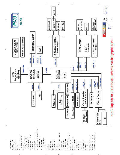
01_Block Diagram
02_System Setting
CPU
03_Power Sequence
04_EC Pin Define
05_History
Celeron-M ULV
(Dothan)
CLOCK GEN
ICS9LPR426
P900
D 06_* FCBGA479 D
07_Clock Gen_ICS9LPR426
THERMAL CONTROL
R1.2G
08_Dothan_HOST FSB400MHz
09_Dothan_PWR_GND
10_910GML_HOST_DMI
11_910GML_DRAM
12_910GML_VGA_LVDS_TV 400MHz
13_910GML_PWR LVDS
NORTH
14_910GML_GND 8.9 AUO LCD BRIDGE Channel A SODIMM 200P
15_ICH6-M_Azalia_GPIO_PCI_LAN
16_ICH6-M_USB_PCIE_DMI_IDE_SATA 910GML 400MHz
17_ICH6-M_PWR_GND
RGB
CRT Channel B NC
18_DDR2 SODIMM
19_DDR2_Termination
20_Onboard VGA
C
21_LCD Conn
x4 DMI C
22_Minicard LINE OUT
23_LAN_Atheros L2
24_RJ45/BlueTooth
25_Onboard Flash Debug Conn AUDIO AMP Speaker
26_Flash Conn
AZALIA AZALIA CODEC
27_USB Port
SOUTH Realtek ALC662
LPC EXT MIC
28_Card Reader_ENE UB6225P EC BRIDGE
29_Camera Conn ENE KBC3310
30_Codec_ALC662 INT MIC
31_Audio_AMP_Jack ICH6-M
32_EC_ENE KB3310 SPI ROM Internal KB Touch Pad
33_Switch_SPI ROM_Debug Conn
34_KB_Touch Pad
B B
35_Thermal Sensor_FAN BlueTooth AW-BT253 USB_P6
36_LED_THERMTRIP
PCIE
37_Discharge USB_P1/2/3
38_PWR Jack USB Port *3 PCIE_3
WLAN
39_Srew Hole USB_P5 MINICARD AW-GE780
40_EMI
41_POWER FLOW SD/MMC Card Reader USB_P4
42_CHARGER
Card Reader ENE UB6225P PCIE_2
43_VCORE(7A)
LAN RJ-45
44_POWER_3V_5V_VTT_DDR Atheros L2
45_POWER_3VA_3VSB
USB_P7
1.3M Camera
46_POWER_1.05V_1.5V_2.5V Onboard
IDE Slave Flash Controller
47_POWER_1.8V_DUAL_5VSB USB_P0 NAND Flash
PHISON
NAND Flash SATA1
A Flash Conn A
Card IDE Master
P900_R1.1G_W/O_FLASH
Title : Block Diagram
HD Engineer: Tiansen_Wu
ASUSTek Computer INC.
Size Project Name Rev
A3 P900 1.2G
Date: Wednesday, February 27, 2008 Sheet 1 of 47
5
http://laptop-motherboard-schematic.blogspot.com/
4 3 2 1
5 4 3 2 1
D ICH6 GPIO SETTING D
Pin Pin Name Connect to Type Input/Output Set
B7 GPI0/REQ6# 10K Pull +3V I fixed as Input only Pin Pin Name Connect to Type Input/Output Set
E8 GPI1 / REQ5# 10K Pull +3V I fixed as Input only AF17 GPI26/SATA0GP NC GPI (GPI)Input
D9 GPI2 / PIRQE# 10K Pull +3V I fixed as Input only R3 GPIO27 CARD_READER_EN# I/O Output
C7 GPI3 / PIRQF# 10K Pull +3V I fixed as Input only T3 GPIO28 NC I/O Output
C6 GPI4 / PIRQG# 10K Pull +3V I fixed as Input only AE18 GPI29 / SATA1GP PCBVER0 GPI (GPI)Input
M3 GPI5 / PIRQH# 10K Pull +3V I fixed as Input only AF18 GPI30 / SATA2GP NC GPI (GPI)Input
AD19 GPI6 / BMBUSY# NB BMBUSY# I Input AG18 GPI31 / SATA3GP PCBVER1 GPI (GPI)Input
AE19 GPI7 NC GPI fixed as Input only AF19 GPIO32 / CLKRUN# 10K Pull +3V I/O Input
R1 GPI8 EC KBC_SCI# GPI fixed as Input only AF20 GPIO33 PM_VCOREL1 I/O Output
C23 GPI9/OC4# 10K Pull +3V I Input AC18 GPIO34 PM_VCOREL2 I/O Output
D23 GPI10/OC5# 10K Pull +3V I Input NA GPIO35 NA NA NA
W6 GPI11 / SMBALERT# S_SMBALERT# I Input NA GPIO36 NA NA NA
M2 GPI12 NC GPI fixed as Input only NA GPIO37 NA NA NA
C C
R6 GPI13 EC EXTSMI# GPI fixed as Input only NA GPIO38 NA NA NA
C25 GPI14/OC6# 10K Pull +3V I Input NA GPIO39 NA NA NA
C24 GPI15 /OC7# 10K Pull +3V I Input F7 GPI40 / REQ4# 10K Pull +3V I Input
D8 GPO16/GTN6# NC O Output P4 GPI41 / LDRQ1# NC I Input
F6 GPO17 / GNT5# NC O Output NA GPIO42 NA NA NA
AC21 GPO18 / STP_PCI# Clock GEN STP_PCI# O Output NA GPIO43 NA NA NA
AB21 GPO19 WLAN_LED# GPO fixed as Output only NA GPIO44 NA NA NA
AD22 GPO20 / STP_CPU# STP_CPU# O Output NA GPIO45 NA NA NA
AD20 GPO21 CAMERA_EN GPO fixed as Output only NA GPIO46 NA NA NA
NA GPIO22 NC NA NA NA GPIO47 NA NA NA
AD21 GPO23 SPEAKER_EN# GPO fixed as Output only E7 GPO48 /GNT4# NC O Output
V3 GPIO24 MINICARD_EN# I/O Output AC25 GPO49 / CPUPWRGD CPU Power Ok O Output
P5 GPIO25 WLAN_ON# I/O Output
B B
A A
P900_R1.1G_W/O_FLASH
Title : System Setting
ASUSTek Computer INC. Engineer: Tiansen_Wu
Size Project Name Rev
A3 P900 1.2G
Date: Wednesday, February 27, 2008 Sheet 2 of 47
5
http://laptop-motherboard-schematic.blogspot.com/
4 3 2 1
5 4 3 2 1
Signal S0/S1 S3 S4/S5 Power
Only Battery VSUS_ON H H L VSB
*This sequence is for Battery Plug-in and no Adapter, Adapter In VSUS_ON H H H VSB
if Adapter Plug-in,the sequence change to: SUSB_ON H L L Main
A/D_DOCK_IN--->AC_BAT_SYS--->+3VA--->VSUS_ON--->+3VSB & +5VSB
SUSC_ON H H L DUAL
--->VSUS_GD--->PM_REMRST#--->PWR_SW#--->PM_PWRBTN--->PM_SUSC#--->PM_SUSB#
D D
4 3 AC_BAT_SYS
2 3 +5VA +3VA +1.8V_DUAL
A/D_DOCK_IN MP2307DN APL5315BI MP2307DN VTT_DDR
Adapter AC_BAT_SYS 13 SUSC_ON RT9173
7 +5V
MAX8724ETI +3VSB 8
2 BAT_CON VSUS_GD
Battery 2*PMBS3904 +5VSB
VSUS_ON
RT8020A 7 +5VSB +2N7002 7 15 +5V
6
14 SUSB_ON SI4835BDY
7 +3VSB 15 +3V
21 14 SUSB_ON SI4835BDY
+VCCP
24 VCORE H_CPURST# +3V
29 15 16 +2.5V
NB 910GM
DOTHAN CPU +5V
C PM_PWROK 15 SI4835BDY C
VID[0..5] 23 26
3 AC_BAT_SYS 16
PLT_RST#
+1.5V
VRM_PWRGD
25
+5V
MP2307DN
15
(PLT_RST# is 34--41 RTCCLK(=1mS)
later than PM_PWROK,H_CPURST# is
(logic AND of 28 1mS after PLT_RST#)
PWROK and
H_PWRGD 27
VRM_PWROK)
3 AC_BAT_SYS 21
VCC_RTC
1 RTCRST#
+ +VCCP 22 VCCP_OK
SB ICH6
BATT 7 MP2307DN DELAY
(160mS after VRM_PWRGD)
AC_BAT_SYS 20
P_VCC_EN_10
28 19 CPU_VRON 2N7002
PM_RSMRST#
PM_PWRBTN#
11 12
PCI_RST#
PM_PWROK
B B
CLK_PCI_EC
PM_SUSC#
PM_SUSB#
22 VCCP_OK CLK_PCIE_ICH
23
CYS28442
9 10 26 CLK_BCLK_CPU
4 +3VA VSUS_GD
8
5 PWR_SW#
13 SUSC_ON
3 AC_BAT_SYS
VSUS_ON
6 24 VCORE
14 SUSB_ON
EC KB3110 14 +5V 22
VCCP_OK
25 VRM_PWRGD VID[0..5]
CPU_VRON 23 ISL6218CRZ
19 VCORE_PG 25 VRM_PWRGD
AND
(55mS after SUSB_ON) 19 CPU_VRON
A A
28 PCI_RST# 28 PLT_RST# 28 PLT_RST#
IDE FLASH
CONTROLLOR LAN P900_R1.1G_W/O_FLASH
ATTANSIC L2 MINICARD
SM223
Title : Power Sequence
ASUSTek Computer INC. Engineer: Tiansen_Wu
Size Project Name Rev
A3 P900 1.2G
Date: Wednesday, February 27, 2008 Sheet 3 of 47
5
http://laptop-motherboard-schematic.blogspot.com/
4 3 2 1
5 4 3 2 1
EC KB3310 GPIO SETTING
Pin No. Pin Name Signal Name Type NOTE Pin No. Pin Name Signal Name Type NOTE EC KB3310 Other Pin SETTING
1 GA20 A20GATE O A20GATE 70 GPO3D LCD_BACKOFF# O LCD_BACKOFF# Pin No. Pin Name Signal Name Type NOTE
2 KBRST# RC_IN# O KBRST# 71 GPO3E CLK_PWRSAVE# O Active when BAT_IN=1 and 3 SERIRQ INT_SERIRQ I/OD 8.2K Pull +3VS
AC_OK=0(Unused)
6 GPIO04 EMAIL_SW# I EMAIL_SW# , * 72 GPO3F PM_BATLOW# O Battery Low Low 4 LFRAME# LPC_FRAME# I
13 PCIRST# PCI_RST# I PCI Reset 73 GPIO40 AC_OK I AC Adaptor Plug in 5 LAD3 LPC_AD3 I/O
D D
14 GPIO07 BAT_EXT O Reserved 74 GPIO41 PM_RSMRST# O 10K Pull GND 7 LAD2 LPC_AD2 I/O
15 GPIO08 EXTSMI# O EXTSMI#, 10K Pull +3VSUS 75 GPIO42 N.C O Reserved 8 LAD1 LPC_AD1 I/O
16 GPIO0A LID_EC# I LID_EC#, * 76 GPIO43 N.C O Reserved 9 VCC +3VA_EC P
17 GPIO0B NC O LCD chip select 77 SCL1 SMB1_CLK I/OD 4.7K Pull +3VA_EC 10 LAD0 LPC_AD0 I/O
18 GPIO0C NC I/O LCD Data 78 SDA1 SMB1_DAT I/OD 4.7K Pull +3VA_EC 11 GND GND P
19 GPIO0D DISTP_SW# I Touch Pad Disabled,* 79 SCL2 SMB2_CLK I/OD 10K Pull +3VS 12 PCICLK CLK_PCI_EC I
20 SCI# KBC_SCI# O KBC_SCI#, 10K Pull +3VSUS 80 SDA2 SMB2_DAT I/OD 10K Pull +3VS 22 VCC +3VA_EC P
21 PWM1 BL_PWM_DA O LCD Light Switch 81 KSO16 N.C O Reserved 24 GND GND P
23 PWM2 BAT_CRITICAL O LCD clock 82 KSO17 N.C O Reserved 33 VCC +3VA_EC P
25 GPIO11 PM_PWRBTN# OD Power Button to SB, * 83 PSCLK1 LCD_SCL O Reserved 35 GND GND P
26 FANPWM1 FAN0_PWM O CPU Fan(Unused) 84 PSDAT1 LCD_SDA O Reserved 37 ECRST# EC_RST# I Add 100K ohm to GND
27 FANPWM2 FAN1_PWM O VGA Fan(Unused) 85 PSCLK2 LCD_CSB O Reserved 67 AVCC +3VACC P
28 FANFB1 FAN0_TACH I CPU FanTach(Unused) 86 PSDAT2 LCD_VSYNC O Reserved 69 AGND AGND P
29 FANFB2 FAN1_TACH I VGA FanTach(Unused) 87 PSCLK3 TP_CLK I/OD 10K Pull +3VS 94 GND GND P
C C
30 GPIO16 E51_TX O RS232 debug port 88 PSDAT3 TP_DAT I/OD 10K Pull +3VS 96 VCC +3VA_EC P
31 GPIO17 E51_RX O Reserved 89 GPIO50 BATSEL_3S O Battery series. Hi:3S, 111 VCC +3VA_EC P
Lo:4S(Unused)
32 GPIO18 PWR_SW# I power button, * 90 GPIO52 CHG_LED_UP# O charger LED 113 GND GND P
34 GPIO19 MAIL_LED# O Mail LED(Unused) 91 GPIO53 CAP_LED# O EC H/W controls 119 RD# SPI_SO I
36 GPIO1A NUM_LED# O EC H/W controls(Unused) 92 GPIO54 PWR_LED_UP O EC H/W blinking 120 WR# SPI_SI O
38 CLKRUN# N.C O Reserved 93 GPIO55 SCRL_LED# O EC H/W controls 112 XCLKI 32KXCLKI I
39 KSO0 KSO0 O For Keyboard interface 95 GPIO56 PWR4G_SW# I * 123 XCLKO 32KXCLKO O
40 KSO1 KSO1 O For Keyboard interface 97 GPXOA00 SPI_MODE# O "HW Strap for SPI Flash deExternal 124 V18R K_V18R Reserved 1uF to GND
Pull Down 100K ohm to GND"
41 KSO2 KSO2 O For Keyboard interface 98 GPXOA01 SUSC_ON O 125 VCC +3VA_EC P
42 KSO3 KSO3 O For Keyboard interface 99 GPXOA02 VSUS_ON O 128 SPICS# SPI_CE# O
43 KSO4 KSO4 O For Keyboard interface 100 GPXOA03 CPU_VRON O
44 KSO5 KSO5 O For Keyboard interface 101 GPXOA04 SUSB_ON O
45 KSO6 KSO6 O For Keyboard interface 102 GPXOA05 PWROK O
46 KSO7 KSO7 O For Keyboard interface 103 GPXOA06 PM_LEVELDOWN# O Reserved
B 47 KSO8 KSO8 O For Keyboard interface 104 GPXOA07 CHG_EN# O Battery charging enabled B
48 KSO9 KSO9 O For Keyboard interface 105 GPXOA08 PRECHG O
49 KSO10 KSO10 O For Keyboard interface 106 GPXOA09 SPI_WP# O
50 KSO11 KSO11 O For Keyboard interface 107 GPX0A10 OP_SD# O Audio OP
51 KSO12 KSO12 O For Keyboard interface 108 GPXOA11 BAT_LEARN O
52 KSO13 KSO13 O For Keyboard interface 109 GPXID0 BATSEL_2P# O Battery parallel. Hi:1P,
Lo:2P~3P
53 KSO14 KSO14 O For Keyboard interface 110 GPXID1 CPU_LEVELDOWN# O Reserved
54 KSO15 KSO15 O For Keyboard interface 112 GPXID2 THRO_CPU O Active if Battery Temperature
is over spec
55 KSI0 KSI0 I For Keyboard interface 114 GPXID3 SUSB# I Pull Down 100K ohm to GND
56 KSI1 KSI1 I For Keyboard interface 115 GPXID4 SUSC# I Pull Down 100K ohm to GND
57 KSI2 KSI2 I For Keyboard interface 116 GPXID5 CPUPWR_GD I 10K Pull +3VS
58 KSI3 KSI3 I For Keyboard interface 117 GPXID6 VSUS_GD I Disabled **
59 KSI4 KSI4 I For Keyboard interface 118 GPXID7 BAT_VOLSEL O Reserved
60 KSI5 KSI5 I For Keyboard interface 121 GPIO57 INTERNET# I *
61 KSI6 KSI6 I For Keyboard interface 126 SPICLK SPI_CLK O SPI Clock
A A
62 KSI7 KSI7 I For Keyboard interface 127 GPIO59 N.C O Reserved
63 AD0 BAT_ICHG I Sense Power Loading
P900_R1.1G_W/O_FLASH
64 AD1 BAT_CONFIG I sense Battery
65 AD2 BAT_SENT I Reserved Title : EC Pin Define
66 AD3 BAT_TS I Reserved ASUSTek Computer INC. Engineer: Tiansen_Wu
Size Project Name Rev
68 GPO3C DOC O Trigger Clock Gen
A3 P900 1.2G
Date: Wednesday, February 27, 2008 Sheet 4 of 47
5
http://laptop-motherboard-schematic.blogspot.com/
4 3 2 1
5 4 3 2 1
P701 CIRCUIT UPDATED HISTORY
Rev Date Description Rev Date Description
1.0G 2007/02/26 S701L Schematic 1.0G Beginning 1.2G 2007/06/30 P701 Schematic 1.2G Beginning
~~
~~
1. Add R174 to short DASP pins of Master IDE device and SLave IDE device
D 2007/03/16 S701L 1.0G Gerber Out 2. Use SB GPIO27 to controll Card Reader UB6225P Power D
3. PR606084.2 connect to +5V to fix LCD flash issue
1.1G 2007/03/24 S701L Schematic 1.1G Beginning
4. Adjust SPEAKER pin define
~~
5. Adjust CHARGE LED and WLAN LED lightness
2007/04/19 S701L 1.1G Gerber Out
6. Use SB GPI 26, 29, 30, 31 for PCB version
1.0G P701(S701L renamed) Schematic 1.0G Beginning 7. Change USB ESD diode for EMI request
2007/04/24
1. PC8054, PR6075 /X to N/A 8. Add Floating GND TP_GND and Spring TP1 & TP2 for EMI request
~~
2. Attansic L2 change to Atheros L2(pin to pin) 9. Change PM_VCOREL1, PM_VCOREL2 default level
3. LC1, LC33 /CAP/X to N/A 10. Add PQ48 to controll +3V_PE to fix WLAN AW-GE780 can't detect issue
4. C87 change to X5R to cost down 11. Power Charger part update circuit for new Adapter
5. L1, L2, L3 change to 56 NH, R5, R6 change to 75 Ohm to pass CRT EA measure 12. Use SB GPI12 to detect LID signal level
6. PR48 change to 22K Ohm, PC35 change to 4700PF to fix no VCORE issue 13. Add H/W THERMTRIP circuit (page 36)
7. PR6074 change to 4.7K Ohm to fix +3VSB OCP issue 14. Add U40 to prevent system auto power on after clear CMOS
8. Clock Gen CY28442-2 change to ICS9LPR367 15. Use SB GPI7 for THRO_CPU
C
9. Phase in Power Level Reduce solution, mark "Taipei0508" 16. Power Charger part update circuit to prevent incorrect Adapter damage boards C
10. Card Reader Socket change to SD Socket 12G25100091E 17. Q1.1, Q2.1 change to +3V
11. Add System FAN circuit 2007/07/06 P701 1.2G Gerber Out
12. Camera change to USB port 7, Minicard change to USB port 5
1.2G 2007/07/26 P701 Schematic 1.3G Beginning
13. Use SB GPIO27 to Enable/Disable Card Reader UB6225P
~~
1. Add R11 for 801
14. Use SB GPIO28 to Enable/Disable Modem
15. Card Reader UB6225P share 48M clock from CLock Gen with SB USB part
16. Add D29 to fix LCD_CSB leakage current issue
17. LC29, LC30 change to 27PF to pass EA crystal measure
18. Change vaule of PR73, PR74, PC56 and add PC60 to adjust the power sequence timing
between Stand By power and RSMRST#
19. Remove USB port 1
20. Add +5V generate +3V_LCD circuit
21. Remove +5V_CHG generate circuit
22. Use SB GPIO33, GPIO34 to controll the level of VCORE
B 23. U31 use APL5315BI-TRL to replace MAX8863TEUK(pin to pin, but reference voltage level B
different)
24. PR59 change to 130K Ohm for both 12V Adapter and 9.8V Adapter
2007/05/22 P701 1.0G Gerber Out
1.1G 2007/05/31 P701 Schematic 1.1G Beginning
~~
1. Remove the 48M clock from CLock Gen to Card Reader UB6225P
2. Clock Gen ICS9LPR367 change to ICS9LPR426
3. Flash Connector increase SATA and USB interface
4. Add Onboard Flash(SM223 + NAND Flash x4)
5. BATT_CON pin 5 connect to GND
6. Q34 pin 1 connect to +3V to fix EC reset issue
7. Remove J1, J2
8. KB pin 28 connect to GND for P701-ISP_CARD
9. Use SB GPO23 to Enable/Disable Audio Amplifier
10. Use SB GPO21 to controll Camera Power
A A
11. Use SB GPIO24 to controll Minicard Power
12. Use SB GPIO25 to Enable/Disable WLAN Ratio P900_R1.1G_W/O_FLASH
13. Atheros L2 and Minicard SMBUS interface directly pull high
14. LCD_CON pin 20 connect to AC_BAT_SYS Title : History
2007/06/07 P701 1.1G Gerber Out ASUSTek Computer INC. Engineer: Tiansen_Wu
Size Project Name Rev
A3 P900 1.2G
Date: Wednesday, February 27, 2008 Sheet 5 of 47
5
http://laptop-motherboard-schematic.blogspot.com/
4 3 2 1
5 4 3 2 1
D D
C C
B B
A A
P900_R1.1G_W/O_FLASH
Title : Blank
ASUSTek Computer INC. Engineer: Tiansen_Wu
Size Project Name Rev
A3 P900 1.2G
Date: Wednesday, February 27, 2008 Sheet 6 of 47
5
http://laptop-motherboard-schematic.blogspot.com/
4 3 2 1
5 4 3 2 1
CR1 1 2 Do Not Stuff +3VSB +3V_CLK
/X
CL1
1 2
CX1
1
1
1
1
1
1
1
1
1
1
1
CLK_XIN 1 2 CLK_XOUT 120Ohm/100Mhz CC1 CC2 CC3 CC4 CC5 CC6 CC7 ◦ Jabse Service Manual Search 2024 ◦ Jabse Pravopis ◦ onTap.bg ◦ Other service manual resources online : Fixya ◦ eServiceinfo