Service Manuals, User Guides, Schematic Diagrams or docs for : clarion PN2591MG clarion_pn2591mg_sch
<< Back | HomeMost service manuals and schematics are PDF files, so You will need Adobre Acrobat Reader to view : Acrobat Download Some of the files are DjVu format. Readers and resources available here : DjVu Resources
For the compressed files, most common are zip and rar. Please, extract files with Your favorite compression software ( WinZip, WinRAR ... ) before viewing. If a document has multiple parts, You should download all, before extracting.
Good luck. Repair on Your own risk. Make sure You know what You are doing.
Image preview - the first page of the document
>> Download clarion_pn2591mg_sch documenatation <<
Text preview - extract from the document
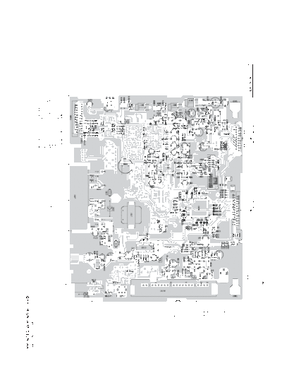
PRINTED WIRING BOARD
Main PWB(B1) section

                                             No.   Description        No.   Description
                                              A    N.C                 I    ILLUMI(+)
                                              B    REAR SP R-CH(+)     J    ACC
                                              C    GND                 K    FRONT SP L-CH(-)
                                              D    REAR SP L-CH(-)     L    FRONT SP R-CH(-)
                                              E    REAR SP L-CH(+)     M    N.C
                                              F    REAR SP R-CH(-)     N    BACK UP
                                              G    FRONT SP L-CH(+)    O    ILLUMI(-)
                                              H    FRONT SP R-CH(+)    P    GND


                                                                                               COMPONENT SIDE


                       - 14 -   PN-2591M-G
Main PWB(B1)) section


         IC506, J701, BL101 are the parts on the component side.


         Caution:
         COMPONENT SIDE: Parts on the component side seen
         from the component side are indicated.                    SOLDER SIDE
         SOLDER SIDE: Parts on the solder side seen
         from the solder side are indicated.


                                                       - 15 -                    PN-2591M-G
CIRCUIT DIAGRAM
Main PWB(B1) 1/2 section


                           - 16 -   PN-2591M-G
◦ Jabse Service Manual Search 2024 ◦ Jabse Pravopis ◦ onTap.bg ◦ Other service manual resources online : Fixya ◦ eServiceinfo