Service Manuals, User Guides, Schematic Diagrams or docs for : honeywell ddp-116 71-293_DDP-116_Interface_Manual_Jan65
<< Back | HomeMost service manuals and schematics are PDF files, so You will need Adobre Acrobat Reader to view : Acrobat Download Some of the files are DjVu format. Readers and resources available here : DjVu Resources
For the compressed files, most common are zip and rar. Please, extract files with Your favorite compression software ( WinZip, WinRAR ... ) before viewing. If a document has multiple parts, You should download all, before extracting.
Good luck. Repair on Your own risk. Make sure You know what You are doing.
Image preview - the first page of the document
>> Download 71-293_DDP-116_Interface_Manual_Jan65 documenatation <<
Text preview - extract from the document
Document No. 71-293
INTERFACE MANUAL
FOR
DDP-116 GENERAL-PURPOSE COMPUTER
January 8, 1965
Prepared by:
Computer Control Company, Inc.
Old Connecticut Path
Framingham, Massachusetts
COPYRIGHT 1965 by Computer Control Company, Incorporated,
Framingham, Massachusetts. Contents of this publication may not
be reproduced in any form, in whole or in part, without permission
of the copyright owner. All rights reserved.
Printed in U. S. A.
CONTENTS
Title Page
Intr oduction 1
DDP-116 1/0 Communication
Standard Parallel 110 Bus 3
Standard 110 Bus Line s 3
Logic Levels 3
OCP Commands 3
SKS Commands 5
INA Commands 6
OTA Commands 6
Standard Interrupt Provisions 7
Gating Circuit Characteristics 8
Direct Multiplexed Channel (DMC) Option 11
110 Transfer s 12
Special DMC Signal Gating Circuit Characteristics 13
Priority Interrupt Option 16
Typical Device Control Interface 17
OCP Commands 17
SKS Testing 17
Standard Input Data Transfer s 17
Standard Output Data Transfers 19
Setting Mask Flip-Flop 19
Standard Interrupt for Input 19
Standard Interrupt for Output 19
System Normalize 20
Special DMC Provisions 20
Parity Check Input 20
System Interconnecting Data 20
Interconnecting Cables 23
1/ 0 Connectors 23
AC Power Distribution 23
DC Power Distribution 23
System Grounding 25
iii
ILLUSTRA TIONS
Figure Title Page
Standard DDP-116
2 DDP-l16 I/O, Block Diagram 2
3 OCP I/O Command, Timing Diagram 5
4 SKS Sensing Command, Timing Diagram 5
5 INA Input Data Transfer, Timing Diagram 6
6 OTA Output Data Transfer, Timing Diagram 7
7 Non-Inverting Power Amplifier PAC, Model PN-30, Schematic
Diagram 8
8 Input Line Termination, Schematic Diag ram 9
9 DMC I/O Transfer, Timing Diagram 14
10 Transfer Gate PAC, Model S-330, Schematic Diagram 16
11 Typical Device Control Interface, Simplified Logic Diagram 18
12 Additional Interface Logic Required for DMC Option 21
13 Rear View of Typical DDP-116 System Installation 22
14 DDP-116 I/O Connectors 24
TABLES
Table Title Page
Single Word Transfer I/O Bus Signal Functions 4
2 ADB07- to ADBI6- and OTBOI to OTB16 Signal Characteristics 10
3 OTPXX -, RRLXX -, OCPXX -, and SMKIX - Signal Characteristics 10
4 INB01- to INBI6- Signal Characteristics 10
5 DRLXX - and PILXX - Signal Characteristics 11
6 ERLXX- and DADI3- through DAD15- Signal Characteristics 15
7 DIL01+ through DIL08+ Signal Characteristics 15
8 Standard I/O Connector A2S lA Pin As signments 25
9 Standard I/O Connector A2S2A Pin As signments 25
10 Standard I/O Connector A2S 1 B Pin Assignments 26
11 Standard I/O Connector A2S2B Pin As signments 26
iv
INTERFACE MANUAL
FOR
DDP-116 GENERAL-PURPOSE COMPUTER
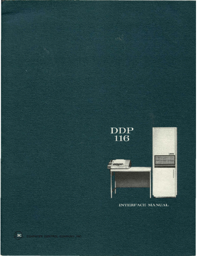
Figure 1. Standard DDP-116
DDP-ll6
INTERFACE MANUAL
INTRODUCTION
The DDP-ll6 General-Purpose Computer (Figure l) features versatile input/output
capabilities, easy expandability through modular design, a variety of input/ output modes,
and simplicity of operation. This manual describes and illustrates the interface character-
istics of the DDP-ll6 to facilitate proper connection with peripheral equipment. The basic
methods of input/output data transfer (Standard I/O Bus and Direct Multiplexed Channel) are
described in sufficient detail for system planning purposes. Data and control lines required
for input/output communications are defined, timing requirements are established, and in-
terface gating drive and load requirements are specified. A detailed description of input/
output operation is given in the DDP-ll6 Programmer I s Manual.
DDP-116 II 0 COMMUNICATION
Communication links between the standard DDP-116 and its peripheral equipment
are illustrated in Figure 2. The standard machine, without options, communicates with
peripheral equipment on a parallel r/o bus under program control. A separate instruction
is required for every input or output word transfer. All peripheral devices (up to 18 may be
attached) are tied to a single interrupt signal line. When a device requests service through
the interrupt line, a programmed subroutine determines which device requires service.
An optional priority interrupt system is available to eliminate the need for programmed
priority determination.
The Direct Multiplexed Channel (DMC) option is a time- shared automatic r/o system
that uses the parallel r/o bus for communication but performs single character or block
data transfers without program intervention. DMC transfers are interleaved with computa-
tion; the starting and terminating addresses of the locations to which the block of information
is to be transferred are set up initially in standard memory locations under program control.
Data transfers thereafter occur at a rate of one word every 6.8 microseconds. The transfer
rate is over 145, 000 words per second. At slower r/o rates, any time not needed by the
DMC is used for computation.
Each peripheral device used with the DDP-116 requires a suitable control interface
compatible with the standard parallel r/o bus. The control interface must be capable of
decoding device addresses and function codes, must provide start- stop and control signals
to the device proper, and in most cases must include a buffer register to synchronize data
transfers with the DDP-116 processing cycle. Control interfaces are provided with all
standard DDP-116 peripheral equipment options. In addition, general-purpose control inter-
faces are available as standard options for use with special devices, or special control in-
1
N
,..-.--- -------------- -- ---------------- - -------- ---STANDARO-iioBUS
'
STOPX
DALOI
I
IK TO 32K I
COINCIDENT RLXX- 1
CURRENT DAL08-
CORE ERLXX-
MEMORY DMC
I
I OPTION I DILOI +
I
I I
I
I I
DIL08+
;_060_ ----- ----t
I
_____ 1__
ARITHMETIC I
REG. I
STANDARD I
(A,B,
DDP-1I6 I
ADDER)
MAIN FRAME :
I
A BUS I
1
I
'- ________ - _____________ - - - - ________ - - ___ - ____ .... _1
'---
--
TO ADDITIONAL
DMC I/O DEVICE
/
CONTROL INTERFACES
Figure 2. DDP-116 r/o, Block Diagram
terfaces can be designed. The following information will enable a user to design any device
or communication link control interface compatible with the DDP-116 bus structure, from
the standpoints of timing, logic levels, and circuit loading.
STANDARD PARALLEL I/O BUS
Standard I/O Bus Lines
The standard DDP-116 input/output mode consists of transfers of single characters
or 16-bit words to and from the data processor B bus. Input transfers are performed by
INA instructions, and output transfers by OTA instructions. Communication with peripheral
device s is accomplished by using an Input/Output Bus, consisting of the following elements:
10 address lines (ADB07 through ADBI6); 16 input data lines (INBOI through INBI6); 16 out-
put data lines (OTBOI through OTBI6); and a series of control lines (OCP, SMK, RRL, OTP,
DRL, and PIL). The data processor distinguishes between devices (with respect to the
destination of commands or the source or destination of data transfers) by a six- bit binary
code on the address bus. Up to 18 devices may be paralleled on the common bus.
Logic Levels
Standard logic levels for S-PAC circuits are 0 volt for logical ZERO and - 6 volts
for logical ONE. Negative logic is used in DDP-116 I/O communication to permit ORing of
r/o bus levels. All active signals (command pulses and binary ONE bits in data and address
codes) are transmitted at the current-driving O-volt level. Binary ZEROs and quiescent
control signals rest at the -6-volt level for minimum current drain.
Timing of the address, data, and command lines from the DDP-116, and timing
requirements imposed on responses from the device control units, are conditional upon the
instruction in effect. Table I provides I/O bus line functions for the operational modes pe-
culiar to I/O processing. Each of the modes is described in detail in the following paragraphs.
OCP Commands
OCP commands initiate motion of a device or prepare it for a specific mode of
operation. No data is exchanged, and no response signal is expected from the addressed
device. Only the address bus lines and the OCPXX-command pulse are involved. OCP
command timing is shown in Figure 3.
The device addres s code and function code are gated from OCP instruction word
positions 7 through 16 to the corresponding bit positions of the address bus. During the
last half of the address interval, the OCPXX-command pulse occurs to enable the addressed
, device to perform the control function specified by the function code portion of the addres s.
No direct response is required of the device. Any information placed by the device on
DRLXX- or INBO I to INB 16 will be ignored by the computer during this instruction.
Execution of the OCP command is verified during the sensing portion of a subsequent SKS,
3
~
Table 1.
Single Word Tra nsfer I/O Bus Signal Functions
Control or Data Function
Line OCP SKS INA OTA Set Mask Interrupt
OTB _ Contains data Contains mask
l 16 status code
INB 1-16 Device applies
data
ADB _ Function code Function code Function code Function code Unique code
7 10
ADB _
ll 16 Device address Device address Device address Device address Unique code
OTP Strobes data to
device buffer
DRL Device replies Device replies Device replies
if condition de- if ready if ready
termined by
function code is
TRUE
RRL Resets device Resets device
ready flip-flop ready flip-flop
OCP Sets mode de-
termined by
function bits
SMK1 Strobes mask
bits to rna-sk
flip-flops
PIL Asynchro-
nous signal
originating
in device I
interface de-
mands pri-
ority interrupt
j
ADB07- THROUGH
ADB 16 - (DEVICE GUARANTEED =:-1
ONE LEVEL (OV) t
'-'0'
ADDRESS AND AT I/O CONNECTOR 1L.._ _ _ _ _ _
ZE_R_0_L_E_V_E_L...;.<-_6_V..;..,)_ _ _--J
FUNCTION CODE)
1013 1210 1980 2190
tt
OV
OCPXX-
GUARANTEED I
AT I/O CONNECTOR I
-6V 11
NOTE: TIME INTERVALS
ARE IN NANOSECONDS
I/O CONNECTOR
TIME REFERENCE
Figure 3. OCP r/o Command, Timing Diagram
INA, or OTA instruction cycle.
Typical uses of the OCP command are to:
a. turn the high- speed paper tape punch on or off,
b. set up the binary or BCD mode in the paper tape reader, and
c. rewind magnetic tape.
SKS Commands
The SKS command is used to te st the condition of any device connected to the
standard I/O bus. The command is implemented by gating the devices address onto the
address bus with a function code that identifies the condition being tested. If the condition
is true, the device interface must bring the DRLXX- line to the O-volt level during the time
limits specified in Figure 4. The DRLXX- signal causes a program skip to the next in-
struction in sequence. If the DRLXX- line remains quiescent, the next instruction in se-
quence is executed.
2281 2455
ADB07-THROUGH
ADB 16 - (DEVICE
GUARANTEED ~ ONE LEVEL (OV) t t
ADDRESS AND AT I/O CONNECTOR 1~___---Z-E-RO-L-E-V-E-L-(---6-V-)---~ __ J
FUNCTION CODE) I
1045 1235
I OV
REQUIREMENT I
DRLXX- MUST ARRIVE BY MUST REMAIN UNTIL
AT I/O CONNECTOR J -6V
+
I/O CONNECTOR
NOTE: TIME INTERVALS
ARE IN NANOSECONDS
TIME REFERENCE
Figure 4. SKS Sensing Command, Timing Diagram
5
INA Com=-"'a..1J.u.;:;
-'~
An INA command addresses a particular device and senses the device condition.
If the device replies with a "ready" indication, the input bus is strobed to the DDP-ll6 A reg-
ister. Timing is illustrated in Figure 5. The address and function code are placed on the
address bus. Within 1. 2 microseconds after receiving the address, the device must bring
the DRLXX-line to the "ready" condition (0 volt level). Otherwise, the DDP-ll6 ignores
the data on the lines and continues with the normal porgram. If the "ready" condition is
detected, data on the input bus is strobed to the A register and the next instruction in
sequence is skipped.
While data is being strobed into the A register, a reset ready pulse (RRLXX-) is
sent out from the computer to indicate that the information has been accepted. This signal
may be used to dc reset the ready flip-flop in the control interface. The device must apply
data to the input bus within 2.3 microseconds after receiving the address.
ADB07- TH ROUGH
ADBI6 -(DEVICE
ADDRESS AND
FUNCTION CODE)
GUARANTEED I
AT I/OCONNEC~ --------~~_ _ _ _ _ _ _ _ _ _ _ _ _ _~
~.
o
ONE LEVEL (OV)
ZERO LEVEL(-6V)
I
1045
3882
t-.. .
_J
,t-----
4055
I
DRLXX- (FROM REQUIREMENT I MUST ARRIVE BY ~--MUST REMAIN UNTIL
DEVICE CONTROL) AT I/O CONNECTOR I
I 2130 2926 3110
I
GUARANTEED I
OV ~
RRLXX- AT I,() CONNECTOR I
-6V
: 1.618 1875
INBOI-THROUGH ~. OV
REQUIREMENT --+I--------------------------~
INBI6-(FROM AT I/O CONNECTO~ MUST ARRIVE BY~ MUST REMAIN UNTIL
DEVICE CONTROL
+ -6V
I/O CON N ECTOR
TI ME REFERENCE NOTE: TIME INTERVALS
ARE IN NANOSECONDS
Figure 5. INA Input Data Transfer, Timing Diagram
OTA Commands
During an OTA output command, the device address and data are applied to the
address and output bus lines. The device's ready status is sensed and if the device is pre-
pared to receive the data, the OT PXX- pulse is generated to strobe the data to the device
buffer. If the device is not ready, no strobing occurs, and the DDP-ll6 program continues
on the assumption that the data transfer was not performed. Timing is illustrated in
Figure 6.
6
ADB07-THROUGH
ADBIS-(DEVICE GUARANTEED:-:-1
ONE LEVEL lOY)
3882 4055
1
f--....;TJ-------
t
ADDRESS AN D AT I/O CONNECTOR~_ _ _ _ _
, Z_E_R_O_L_E_V_E_L....;(_-_S_V..;.)_ _ _ _ _ _ _ _ _ _ _ _- - - - . J J
FUNCTION CODE) I 40 3255 3455
~ ~ ◦ Jabse Service Manual Search 2024 ◦ Jabse Pravopis ◦ onTap.bg ◦ Other service manual resources online : Fixya ◦ eServiceinfo