Service Manuals, User Guides, Schematic Diagrams or docs for : . Electronic Components Datasheets Active components Transistors CET ceh2609
<< Back | HomeMost service manuals and schematics are PDF files, so You will need Adobre Acrobat Reader to view : Acrobat Download Some of the files are DjVu format. Readers and resources available here : DjVu Resources
For the compressed files, most common are zip and rar. Please, extract files with Your favorite compression software ( WinZip, WinRAR ... ) before viewing. If a document has multiple parts, You should download all, before extracting.
Good luck. Repair on Your own risk. Make sure You know what You are doing.
Image preview - the first page of the document
>> Download ceh2609 documenatation <<
Text preview - extract from the document
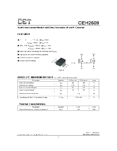
                                                                                                     CEH2609
Dual Enhancement Mode Field Effect Transistor (N and P Channel)


FEATURES

  20V, 3.5A, RDS(ON) = 60m @VGS = 4.5V.
              RDS(ON) = 80m @VGS = 2.5V.
  -20V, -2.5A, RDS(ON) = 100m @VGS = -4.5V.
               RDS(ON) = 145m @VGS = -2.5V.
  Super high dense cell design for extremely low RDS(ON).

  High power and current handing capability.                                                               D1(6)            D2(4)


  Lead free product is acquired.
                                                         4
  Surface mount Package.                             5
                                                 6                                       G1(1)                     G2(3)

                                                                                   3
                                                                               2
                                                                           1                               S1(5)            S2(2)

                                                             TSOP-6


ABSOLUTE MAXIMUM RATINGS                             TA = 25 C unless otherwise noted
                      Parameter                              Symbol                    N-Channel          P-Channel        Units
  Drain-Source Voltage                                            VDS                     20                   -20          V
  Gate-Source Voltage                                             VGS
◦ Jabse Service Manual Search 2024 ◦ Jabse Pravopis ◦ onTap.bg ◦ Other service manual resources online : Fixya ◦ eServiceinfo