Service Manuals, User Guides, Schematic Diagrams or docs for : . Electronic Components Datasheets Active components Transistors GSME 2sk3018
<< Back | HomeMost service manuals and schematics are PDF files, so You will need Adobre Acrobat Reader to view : Acrobat Download Some of the files are DjVu format. Readers and resources available here : DjVu Resources
For the compressed files, most common are zip and rar. Please, extract files with Your favorite compression software ( WinZip, WinRAR ... ) before viewing. If a document has multiple parts, You should download all, before extracting.
Good luck. Repair on Your own risk. Make sure You know what You are doing.
Image preview - the first page of the document
>> Download 2sk3018 documenatation <<
Text preview - extract from the document
Guilin Strong Micro-Electronics Co.,Ltd.
2SK3018
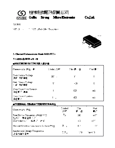
SOT-23 (SOT-23 Field Effect Transistors)
N-Channel Enhancement-Mode MOS FETs
N MOS
MAXIMUM RATINGS
Characteristic Symbol Max Unit
Drain-Source Voltage
BVDSS 35 V
-
Gate- Source Voltage
VGS +20 V
-
Drain Current (continuous)
IDR 100 mA
-
Drain Current (pulsed)
IDRM 400 mA
-
THERMAL CHARACTERISTICS
Symbol Max Unit
Characteristic
Total Device Dissipation PD 200 mW
TA=25 25
Derate above25 25 1.8 mW/
Thermal Resistance Junction to Ambient RJA 417 /W
Junction and Storage Temperature
TJ,Tstg 150,-55to+150
Guilin Strong Micro-Electronics Co.,Ltd.
2SK3018
DEVICE MARKING
2SK3018=KN
2SK3018=
ELECTRICAL CHARACTERISTICS
(TA=25 unless otherwise noted 25)
Characteristic Symbol Min Typ Max Unit
Drain-Source Breakdown Voltage
BVDSS 35 -- -- V
-(ID =10uA ,VGS=0V)
Gate Threshold Voltage
VGS(th) 0.8 -- 2 V
(ID =100uA ,VGS= VDS)
Drain-Source On Voltage
-(ID=50mA ,VGS=5V) VDS(ON) -- -- 0.375 V
(ID =400mA ,VGS=10V) 3.75
Diode Forward Voltage Drop
VSD -- -- 1.5 V
(ISD=200mA ,VGS=0V)
Zero Gate Voltage Drain Current
(VGS=0V, VDS= BVDSS) IDSS -- -- 1 uA
(VGS=0V, VDS=0.8BVDSS, TA=125) 500
Gate Body Leakage
IGSS -- -- +100 nA
(VGS=+20V, VDS=0V)
Static Drain-Source On-State Resistance
(ID=50mA ,VGS=4.5V) RDS(ON) -- -- 8
(ID=400mA ,VGS=10V) 7.5
Input Capacitance
CISS -- -- 50 pF
(VGS=0V, VDS=25V,f=1MHz)
Common Source Output Capacitance
(VGS=0V, VDS=25V,f=1MHz) COSS -- -- 25 pF
Turn-ON Time
t(on) -- -- 20 ns
(VDS=30V, ID=200mA, RGEN=25)
Turn-OFF Time
t(off) -- -- 40 ns
(VDS=30V, ID=200mA, RGEN=25)
Reverse Recovery Time
(ISD=800mA, VGS=0V) trr -- 400 -- ns
1. FR-5=1.0◦ Jabse Service Manual Search 2024 ◦ Jabse Pravopis ◦ onTap.bg ◦ Other service manual resources online : Fixya ◦ eServiceinfo