Service Manuals, User Guides, Schematic Diagrams or docs for : . Electronic Components Datasheets Active components Transistors Fairchild Semiconductor fdc6304p
<< Back | HomeMost service manuals and schematics are PDF files, so You will need Adobre Acrobat Reader to view : Acrobat Download Some of the files are DjVu format. Readers and resources available here : DjVu Resources
For the compressed files, most common are zip and rar. Please, extract files with Your favorite compression software ( WinZip, WinRAR ... ) before viewing. If a document has multiple parts, You should download all, before extracting.
Good luck. Repair on Your own risk. Make sure You know what You are doing.
Image preview - the first page of the document
>> Download fdc6304p documenatation <<
Text preview - extract from the document
July 1997
FDC6304P
Digital FET, Dual P-Channel
General Description Features
These P-Channel enhancement mode field effect transistor are -25 V, -0.46 A continuous, -1.0 A Peak.
produced using Fairchild's proprietary, high cell density, DMOS RDS(ON) = 1.5 @ VGS= -2.7 V
technology. This very high density process is tailored to minimize RDS(ON) = 1.1 @ VGS = -4.5 V.
on-state resistance at low gate drive conditions. This device is
designed especially for application in battery power applications Very low level gate drive requirements allowing direct
such as notebook computers and cellular phones. This device operation in 3V circuits. VGS(th) < 1.5 V.
has excellent on-state resistance even at gate drive voltages as
low as 2.5 volts. Gate-Source Zener for ESD ruggedness.
>6kV Human Body Model.
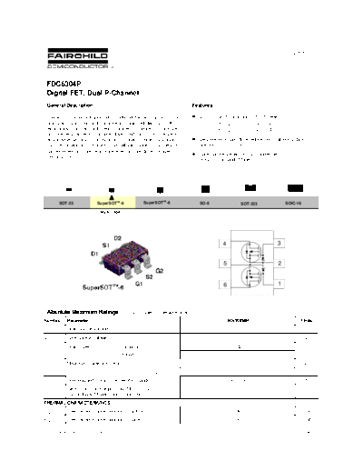
SOT-23 SuperSOTTM-6 SuperSOTTM-8 SO-8 SOT-223 SOIC-16
Mark: .304
4 3
5 2
6 1
Absolute Maximum Ratings TA = 25oC unless other wise noted
Symbol Parameter FDC6304P Units
VDSS Drain-Source Voltage -25 V
VGSS Gate-Source Voltage -8 V
ID Drain Current - Continuous -0.46 A
- Pulsed -1
PD Maximum Power Dissipation (Note 1a) 0.9 W
(Note 1b) 0.7
TJ,TSTG Operating and Storage Temperature Range -55 to 150 ◦ Jabse Service Manual Search 2024 ◦ Jabse Pravopis ◦ onTap.bg ◦ Other service manual resources online : Fixya ◦ eServiceinfo