Service Manuals, User Guides, Schematic Diagrams or docs for : . Electronic Components Datasheets Active components Transistors Fairchild Semiconductor fdg6301n
<< Back | HomeMost service manuals and schematics are PDF files, so You will need Adobre Acrobat Reader to view : Acrobat Download Some of the files are DjVu format. Readers and resources available here : DjVu Resources
For the compressed files, most common are zip and rar. Please, extract files with Your favorite compression software ( WinZip, WinRAR ... ) before viewing. If a document has multiple parts, You should download all, before extracting.
Good luck. Repair on Your own risk. Make sure You know what You are doing.
Image preview - the first page of the document
>> Download fdg6301n documenatation <<
Text preview - extract from the document
July 1999
FDG6301N
Dual N-Channel, Digital FET
General Description Features
These dual N-Channel logic level enhancement mode 25 V, 0.22 A continuous, 0.65 A peak.
field effect transistors are produced using Fairchild's RDS(ON) = 4 @ VGS= 4.5 V,
proprietary, high cell density, DMOS technology. This RDS(ON) = 5 @ VGS= 2.7 V.
very high density process is especially tailored to
minimize on-state resistance. This device has been Very low level gate drive requirements allowing direct
designed especially for low voltage applications as a operation in 3 V circuits (VGS(th) < 1.5 V).
replacement for bipolar digital transistors and small
Gate-Source Zener for ESD ruggedness
signal MOSFETs. (>6kV Human Body Model).
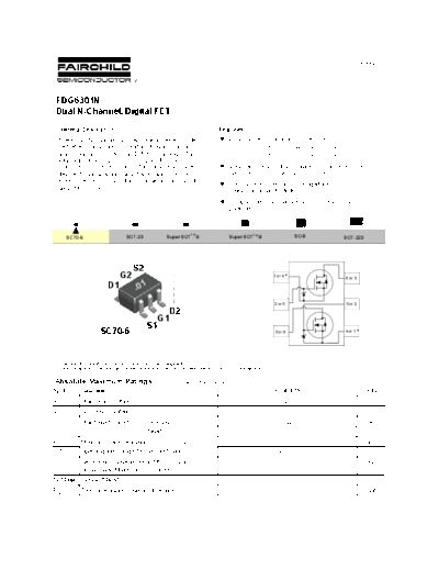
Compact industry standard SC70-6 surface mount
package.
SC70-6 SOT-23 SuperSOTTM-6 SuperSOTTM-8 SO-8 SOT-223
S2
G2 1 or 4 *
6 or 3
D1 .01
2 or 5 5 or 2
D2
G1
S1
SC70-6 3 or 6 4 or 1 *
*The pinouts are symmetrical; pin 1 and 4 are interchangeable.
Units inside the carrier can be of either orientation and will not affect the functionality of the device.
Absolute Maximum Ratings TA = 25◦ Jabse Service Manual Search 2024 ◦ Jabse Pravopis ◦ onTap.bg ◦ Other service manual resources online : Fixya ◦ eServiceinfo