Service Manuals, User Guides, Schematic Diagrams or docs for : . Electronic Components Datasheets Active components Transistors Fairchild Semiconductor fds6690
<< Back | HomeMost service manuals and schematics are PDF files, so You will need Adobre Acrobat Reader to view : Acrobat Download Some of the files are DjVu format. Readers and resources available here : DjVu Resources
For the compressed files, most common are zip and rar. Please, extract files with Your favorite compression software ( WinZip, WinRAR ... ) before viewing. If a document has multiple parts, You should download all, before extracting.
Good luck. Repair on Your own risk. Make sure You know what You are doing.
Image preview - the first page of the document
>> Download fds6690 documenatation <<
Text preview - extract from the document
February 1997
PRELIMINARY
FDS6690
Single N-Channel Logic Level PWM Optimized PowerTrench MOSFET
General Description Features
This N Channel Logic Level MOSFET has been designed 10 A, 30 V. RDS(ON) = 0.0135 @ VGS = 10 V
specifically to improve the overall efficiency of DC/DC RDS(ON) = 0.0200 @ VGS = 4.5 V.
converters using either synchronous or conventional switching
PWM controllers. Optimized for use in switching DC/DC converters with
The MOSFET features faster switching and lower gate charge PWM controllers.
than other MOSFETs with comparable RDS(ON) specifications.
Very fast switching .
The result is a MOSFET that is easy and safer to drive (even at
very high frequencies), and DC/DC power supply designs with Low gate charge (Qg typ = 13 nC).
higher overall efficiency.
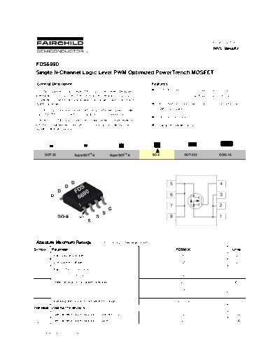
SOT-23 SuperSOTTM-6 SuperSOTTM-8 SO-8 SOT-223 SOIC-16
D 5 4
D S
D FD 9 0
6 3
D 66
7 2
G
S
SO-8 pin 1 S 8 1
S
Absolute Maximum Ratings TA = 25oC unless other wise noted
Symbol Parameter FDS6690 Units
VDSS Drain-Source Voltage 30 V
VGSS Gate-Source Voltage ◦ Jabse Service Manual Search 2024 ◦ Jabse Pravopis ◦ onTap.bg ◦ Other service manual resources online : Fixya ◦ eServiceinfo