Service Manuals, User Guides, Schematic Diagrams or docs for : . Electronic Components Datasheets Active components Transistors Fairchild Semiconductor fds8934a

<< Back | Home

Most service manuals and schematics are PDF files, so You will need Adobre Acrobat Reader to view : Acrobat Download Some of the files are DjVu format. Readers and resources available here : DjVu Resources
For the compressed files, most common are zip and rar. Please, extract files with Your favorite compression software ( WinZip, WinRAR ... ) before viewing. If a document has multiple parts, You should download all, before extracting.
Good luck. Repair on Your own risk. Make sure You know what You are doing.


Image preview - the first page of the document
fds8934a


>> Download fds8934a documenatation <<

Text preview - extract from the document
                                                                                                                                         May 1998


  FDS8934A
  Dual P-Channel Enhancement Mode Field Effect Transistor
  General Description                                                                   Features

     SO-8 P-Channel enhancement mode power field effect                                    -4 A , -20 V, RDS(ON) = 0.055  @ VGS = -4.5 V,
     transistors are produced using Fairchild's proprietary, high                                        RDS(ON) = 0.072  @ VGS = -2.5 V.
     cell density, DMOS technology. This very high density
     process is especially tailored to minimize on-state resistance                        High density cell design for extremely low RDS(ON).
     and provide superior switching performance. These devices
     are particularly suited for low voltage applications such as                          High power and current handling capability in a widely
     notebook computer power management and other battery                                  used surface mount package.
     powered circuits where fast switching, low in-line power loss,                        Dual MOSFET in surface mount package.
     and resistance to transients are needed.


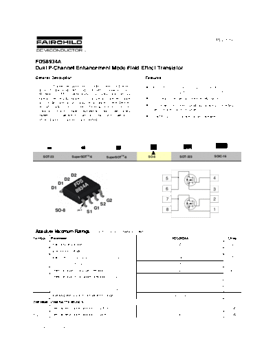
         SOT-23                    SuperSOTTM-6                SuperSOTTM-8              SO-8                 SOT-223                SOIC-16


                                  D2
                            D2                                                                      5                                4
                      D1                 S
                D1
                                      FD 4A
                                         3                                                          6                                3
                                       89
                                                               G2                                   7                                2
                                                          S2
                                                     G1                                             8                                1
                    SO-8                pin 1
                                                S1


  Absolute Maximum Ratings                           TA = 25oC unless otherwise noted
Symbol          Parameter                                                                               FDS8934A                                 Units
VDSS            Drain-Source Voltage                                                                        -20                                   V
VGSS            Gate-Source Voltage                                                                          -8                                   V
ID              Drain Current - Continuous                           (Note 1a)                               -4                                   A
                                  - Pulsed                                                                  -20
PD              Power Dissipation for Dual Operation                                                         2                                    W
                Power Dissipation for Single Operation              (Note 1a)                               1.6
                                                                    (Note 1b)                                1
                                                                    (Note 1c)                               0.9
TJ,TSTG         Operating and Storage Temperature Range                                                  -55 to 150                               


◦ Jabse Service Manual Search 2024 ◦ Jabse PravopisonTap.bg ◦ Other service manual resources online : FixyaeServiceinfo