Service Manuals, User Guides, Schematic Diagrams or docs for : . Electronic Components Datasheets Active components Transistors KEC mpsa55

<< Back | Home

Most service manuals and schematics are PDF files, so You will need Adobre Acrobat Reader to view : Acrobat Download Some of the files are DjVu format. Readers and resources available here : DjVu Resources
For the compressed files, most common are zip and rar. Please, extract files with Your favorite compression software ( WinZip, WinRAR ... ) before viewing. If a document has multiple parts, You should download all, before extracting.
Good luck. Repair on Your own risk. Make sure You know what You are doing.


Image preview - the first page of the document
mpsa55


>> Download mpsa55 documenatation <<

Text preview - extract from the document
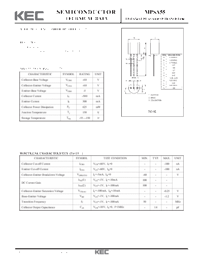
                                   SEMICONDUCTOR                                                                       MPSA55
                                            TECHNICAL DATA                                EPITAXIAL PLANAR PNP TRANSISTOR


  AUDIO FREQUENCY AMPLIFIER APPLICATIONS.

                                                                                                   B                             C

  FEATURES
    Complementary to MPSA05.


                                                                                                                       A
    Driver Stage Application of 20 to 25 Watts Amplifiers.
                                                                                                                                      N    DIM       MILLIMETERS
                                                                                                                   E                        A         4.70 MAX
                                                                                           K
                                                                                                           G                                B         4.80 MAX
                                                                                           D                                                C         3.70 MAX


                                                                                                                       J
                                                                                                                                            D             0.45
                                                                                                                                            E             1.00
  MAXIMUM RATING (Ta=25                 )                                                                                                   F             1.27
                                                                                                                                            G             0.85
         CHARACTERISTIC                 SYMBOL       RATING       UNIT                                                                      H             0.45
                                                                                                       H                                    J               _
                                                                                                                                                      14.00 + 0.50
    Collector-Base Voltage                  VCBO        -60        V                       F                   F                            K         0.55 MAX
                                                                                                                                            L             2.30
    Collector-Emitter Voltage               VCEO        -60        V                                                                        M         0.45 MAX
                                                                                                                                            N            1.00


                                                                                                                       C
                                                                                               1   2   3
    Emitter-Base Voltage                    VEBO            -5     V


                                                                                       L


                                                                                                                   M
                                                                                                                            1. EMITTER
    Collector Current                        IC         -500       mA                                                       2. BASE
                                                                                                                            3. COLLECTOR
    Emitter Current                          IE         500        mA
    Collector Power Dissipation              PC         625       mW
    Junction Temperature                     Tj         150                                                                 TO-92
    Storage Temperature                     Tstg     -55 150


  ELECTRICAL CHARACTERISTICS (Ta=25                     )
               CHARACTERISTIC                       SYMBOL               TEST CONDITION                            MIN.        TYP.        MAX.             UNIT
    Collector Cut-off Current                        ICBO        VCB=-60V, IE=0                                        -          -         -100             nA
    Emitter Cut-off Current                           ICEO       VCE=-60V, IB=0                                        -          -         -100             nA
    Collector-Emitter Breakdown Voltage             V(BR)CEO     IC=-5mA, IB=0                                     -60            -              -            V
                                                     hFE(1)      VCE=-1V, IC=-10mA                                 100            -              -
    DC Current Gain
                                                     hFE(2)      VCE=-1V, IC=-100mA                                100            -              -
    Collector-Emitter Saturation Voltage            VCE(sat)     IC=-100mA, IB=-10mA                                   -          -         -0.25             V
    Base-Emitter Voltage                              VBE        VCE=-1V, IC=-100mA                                    -          -          -1.2             V
    Transition Frequency                               fT        VCE=-1V, IC=-100mA                                    50         -              -          MHz
    Collector Output Capacitance                      Cob        VCB=-10V, IE=0, f=1MHz                                -         14              -           pF


1999. 11. 30                      Revision No : 3                                                                                                                    1/1


◦ Jabse Service Manual Search 2024 ◦ Jabse PravopisonTap.bg ◦ Other service manual resources online : FixyaeServiceinfo